Sundance SMT702 User Manual
Page 50
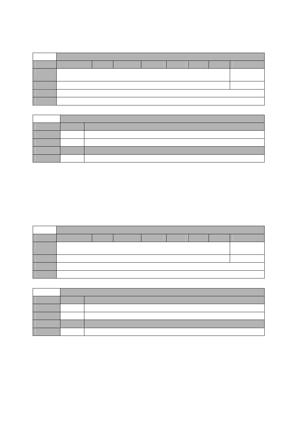
4.3.1.2.29
ADCA – DCM Phase Shift – 0x108 (write).
Offset 0x0400 –
ADCA – DCM Phase Shift – 0x108 (write).
Byte
Bit 7
Bit 6
Bit 5
Bit 4
Bit 3
Bit 2
Bit 1
Bit 0
1
Phase Shift
Sign
Default
‘0’
0
Phase Shift[7:0]
Default
‘00000000’
Offset 0x0400 -
ADCA – DCM Phase Shift – 0x108 (write)
Setting
Bit 8
Sign of Phase Shift
0
0x0
Positive phase shift
1
0x1
Negative phase shift
Setting
Bit 7-0
Phase Shift value
0
8-bit phase shift value to describe a phase shift between 0 and 255
The default firmware implements one DCM_ADV (see Xilinx Virtex 5 documentation
for more details) per ADC data path, i.e. one DCM_ADV for ADCA and one for ADCB.
Both are set to have a programmable phase shift, which means it can be changed
from the host application. Both DCMs are set in mode VARIABLE_CENTER.
There is one bit to set the sign of the phase shit and 8 bit to set the value. The phase
shift range is -255…+255. Once the control word of send, the DCM is being reset
and programmed with the new phase shift. By default, the shift register is set to 0.
4.3.1.2.30
ADCB – DCM Phase Shift – 0x10C (write).
Offset 0x0400 –
ADCB – DCM Phase Shift – 0x10C (write).
Byte
Bit 7
Bit 6
Bit 5
Bit 4
Bit 3
Bit 2
Bit 1
Bit 0
1
Phase Shift
Sign
Default
‘0’
0
Phase Shift[7:0]
Default
‘00000000’
Offset 0x0400 -
ADCB – DCM Phase Shift – 0x10C (write)
Setting
Bit 8
Sign of Phase Shift
0
0x0
Positive phase shift
1
0x1
Negative phase shift
Setting
Bit 7-0
Phase Shift value
0
8-bit phase shift value.
The default firmware implements one DCM_ADV per ADC data path, i.e. one
DCM_ADV for ADCA and one for ADCB. Both are set to have a programmable phase
shift, which means it can be changed from the host application. Both DCMs are set
in mode VARIABLE_CENTER.