Sundance SMT702 User Manual
Page 33
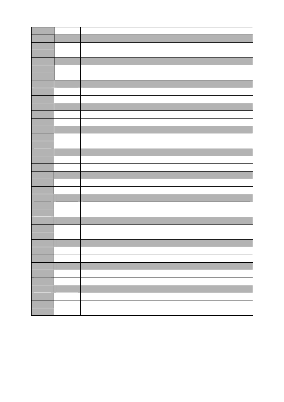
1
1
Normal Mode of Operation.
Setting
Bit 20
Description – DDR2 fifo empty. Memory Bank B.
0
0
DDR2 fifo contains samples.
1
1
DDR2 fifo is empty.
Setting
Bit 21
Description – IDelay Control Ready. Memory Bank B.
0
0
A problem occurred or Memory Bank B is kept in reset.
1
1
Normal Mode of Operation.
Setting
Bit 22
Description – DDR2 Fifo Ready. Memory Bank B.
0
0
Fifo not ready. Data should not be written.
1
1
Normal Mode of Operation.
Setting
Bit 23
Description – DDR2 Fifo Full. Memory Bank A
0
0
Memory bank A not full.
1
1
Memory bank A full.
Setting
Bit 24
Description – DDR2 Fifo Full. Memory Bank B
0
0
Memory bank B not full.
1
1
Memory bank B full.
Setting
Bit 25
Description – DDR2 Fifo almost empty. Memory Bank A
0
0
Memory bank A not almost empty.
1
1
Memory bank A almost empty.
Setting
Bit 26
Description – DDR2 Fifo almost empty. Memory Bank B
0
0
Memory bank B not almost empty.
1
1
Memory bank B almost empty.
Setting
Bit 27
Description – System Monitor – FPGA Die Temperature Alarm
0
0
Normal Mode of Operation.
1
1
Upper die temperature threshold reached.
Setting
Bit 28
Description – System Monitor – Vccint Alarm
0
0
Normal Mode of operation.
1
1
Upper Vccint threshold reached.
Setting
Bit 29
Description – System Monitor – Vccaux Alarm
0
0
Normal Mode of Operation.
1
1
Upper Vccaux threshold reached.
Setting
Bit 30
Description – ADCa synch reference state
0
0
The clock coming out of ADCa is at a low logic level at the time it’s been scanned.
1
1
The clock coming out of ADCa is at a high logic level at the time it’s been scanned.
Setting
Bit 31
Description – ADCb synch reference state
0
0
The clock coming out of ADCb is at a low logic level at the time it’s been scanned.
1
1
The clock coming out of ADCb is at a high logic level at the time it’s been scanned.