3 fpga design – Sundance SMT702 User Manual
Page 28
4.3
FPGA Design
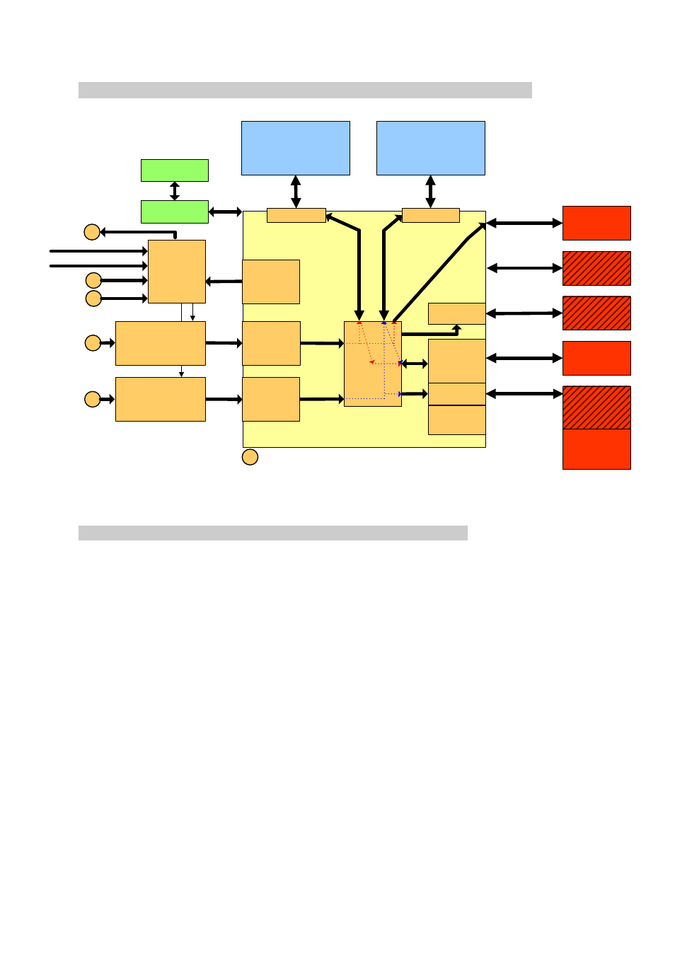
The following block diagram shows how the default FPGA design is organised.
\
Flash
DDR2 Memory BankA
64-bit wide
1Gbytes, 250MHz
CPLD
4x8 bits
(375MHz)
DDR
LVDS
4x8 bits
(375MHz)
DDR
LVDS
DDR2 Memory BankB
64-bit wide
1Gbytes, 250MHz
#2
#1
ADCA (8-bit,
3GSPS)
ADC083000
National Semiconductor
#3
Ext Clk
#4
Ext Ref
Clock
Distribution
LMX2531
Virtex 5 LXT
ADCB (8-bit,
3GSPS)
ADC083000
National Semiconductor
8x8 bits
(187.5 MHz)
DDR
LVDS
8x8 bits
(187.5 MHz)
DDR
LVDS
PCI
Express
Core
(Endpoint)
DDR2 Interface
DDR2 Interface
RSL
Interface
8
x
8
b
it
s
(
1
8
7
.5
M
H
z
)
D
D
R
L
V
D
S
8
x
8
b
it
s
(
1
8
7
.5
M
H
z
)
D
D
R
L
V
D
S
ADC and
Clock SPIs
Control
Registers
Demux
1:2
Demux
1:2
1 - Note that all blocks are control by the Register Block. Command
are received from the PXIe bus and decoded.
2 – Samples are stored directly in the memory and played back to
be sent over PXIe, RSL, optionally SATA or optionally PCI
2xlanes
Dual SATA
connector
(optional)
4 PXIe Lanes
Data&Control
PXIe
Bus
4xlanes
4xRSL
via RSL connectors
#x
SMA connector on
the front panel
32-bit PXI/SHB
32-bit PXI
Bus
(optional)
PCI Interface
(opt)
PXIe Ref (100MHz)
PXI Ref (10MHz)
#5
Ref Out
DDR
SHB(ChA)
connector
32-bit SHB
4x
8
bi
ts
(3
75
M
H
z)
D
D
R
4x8
bits
(375
MHz)
DDR
or DDR SHB
(ChB)
connector
(standard SMT702)
Figure 13 - Block Diagram - FPGA Design (standard Firmware).
4.3.1
Control Registers
The Control Registers drive the complete functionality of the SMT702. They are
setup via the PXIe bus (standard firmware provided). The settings of the ADCs,
triggers, clocks and the configuration of the RSL/PXI interfaces (optional SATA) and
the internal FPGA data path settings can be configured.
The data passed on to the SMT702 over the PXIe bus must conform to a certain
packet structure and to specific addresses and offsets. Only valid packets will be.
4.3.1.1
Memory Map
The write packets must contain the address where the data must be written to and
the read packets must contain the address where the required data must be read.
The following figure shows the memory map for the writable and readable registers
on the SMT702:
The access to a specific register is made by reading or writing to the address:
Address from Host = Offset + Register Address