2 a/d data & channel registers – Measurement Computing CIO-DAS16Jr/16 User Manual
Page 16
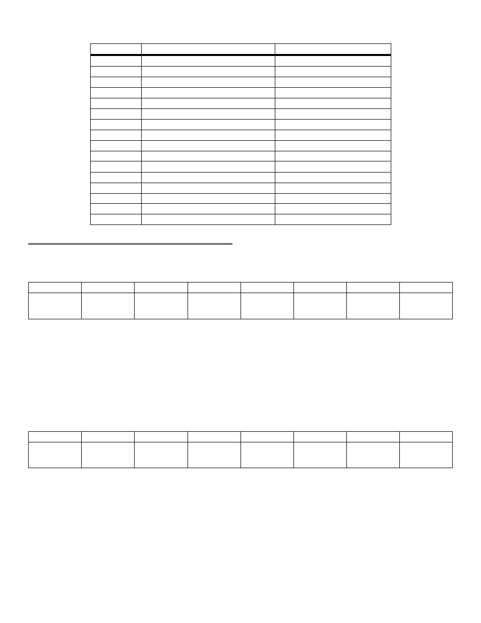
Table 3-2. Register Summary
Pacer Clock Contol (8254)
None. No read back on 8254
BASE + 15
CTR 2 Data - A/D Pacer
CTR 2 Data - A/D Pacer Clock
BASE + 14
CTR 1 Data - A/D Pacer
CTR 1 Data - A/D Pacer Clock
BASE + 13
Counter 0 Data
Counter 0 Data
BASE + 12
Gain control
Gain setting read-back
BASE + 11
None
Pacer clock control register.
BASE + 10
Set DMA, INT etc
DMA, Interrupt & Trigger Control
BASE + 9
None
Status EOC, UNI/BIP etc.
BASE + 8
None
None
BASE + 7
None
None
BASE + 6
None
None
BASE + 5
None
None
BASE + 4
Digital 4 Bit Output
Digital 4 Bit Input
BASE + 3
Channel MUX Set
Channel MUX Read
BASE + 2
None
A/D Bits 1 (MSB) - 8
BASE + 1
Start A/D Function
A/D Bits 9 - 16 (LSB)
BASE
WRITE FUNCTION
READ FUNCTION
ADDRESS
3.2 A/D DATA & CHANNEL REGISTERS
BASE ADDRESS
A/D16
LSB
A/D15
A/D14
A/D13
A/D12
A/D11
A/D10
A/D9
0
1
2
3
4
5
6
7
A read/write register.
READ
On read, it contains the 8LSB’s of A/D data.
WRITE
Writing any data to the register causes an immediate A/D conversion.
BASE ADDRESS + 1
A/D8
A/D7
A/D6
A/D5
A/D4
A/D3
A/D2
A/D1
MSB
0
1
2
3
4
5
6
7
A Read-only register.
On read the most significant A/D byte is read.
12