3 channel mux hi/lo limits word register – Measurement Computing CIO-DAS6402/12 User Manual
Page 20
A/D DATA WORD REGISTER - 16 BIT
BASE + 0
Example, 300h, 768 Decimal
READ/WRITE
AD0
LSB
AD1
AD2
AD3
AD4
AD5
AD6
AD7
AD8
AD9
AD10
AD11
AD12
AD13
AD14
AD15
MSB
COMPATIBLE
AD0
LSB
AD1
AD2
AD3
AD4
AD5
AD6
AD7
AD8
AD9
AD10
AD11
AD12
AD13
AD14
AD15
MSB
ENHANCED
0
1
3
2
4
5
6
7
8
9
10
11
12
13
14
15
Mode
READ
On read, the 16-bit ADC value is presented in 'left-justified' format, with the most-significant ADC bit occupying the data word
bit position #15; the least-significant ADC bit occupies bit position #0 of the data word.
WRITE
A write to the base address will cause an A/D conversion, (Bits 0&1 of BASE+9 must be 0.)
Whether in ENHANCED or COMPATIBLE MODE, there is no channel tag.
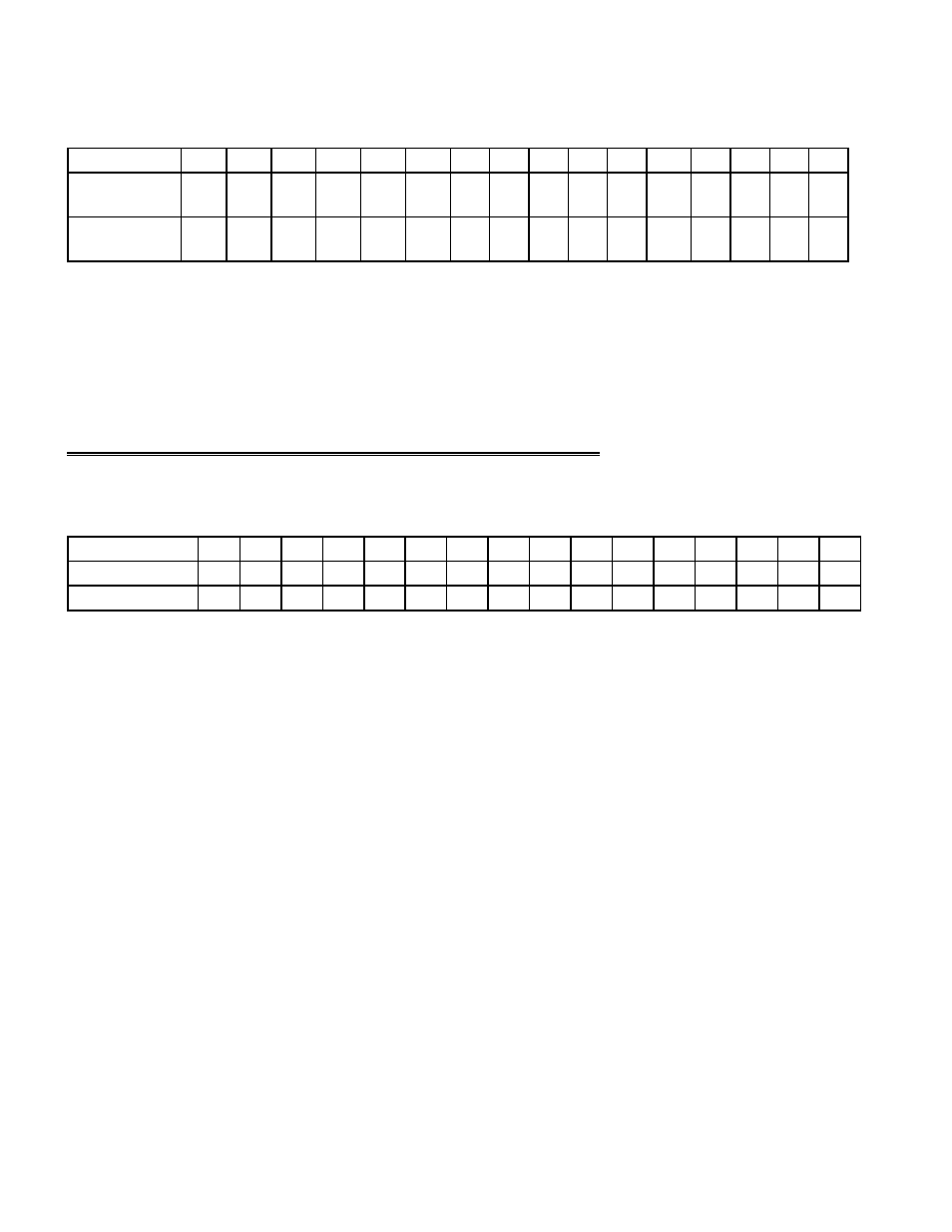
5.3
CHANNEL MUX HI/LO LIMITS WORD REGISTER
BASE ADDRESS +2
Example, 302h, 770 Decimal
WRITE
1L
2L
4L
8L
1H
2H
4H
8H
-
-
-
-
-
-
-
-
COMPATIBLE
LO0
LO1
LO2
LO3
LO4
LO5
-
-
HI 0
HI 1
HI 2
HI 3
HI 4
HI 5
-
-
ENHANCED
0
1
3
2
4
5
6
7
8
9
10
11
12
13
14
15
Mode
WRITE
Writing to this register clears the FIFO.
ENHANCED MODE:
This register is configured as a Word to allow for additional bits, two for the low channel limit and two for the high channel limit,
which are used to generate the 6-bit counter sequence. This register cannot be accessed as two separate byte writes, access must
be done as an entire word. If a byte write to address 302 is attempted, then the HI0-HI5 data will be undefined. If a byte write to
address 303 is attempted, the board will assume that the data is to be written to the DOUT register.
When this register is written, the analog input multiplexers are set to the channel specified in LO0-LO5. After each conversion, the
input multiplexers increment to the next channel, reloading to the "LO" channel after the "HI" channel is reached.
READ
Used to return the pre-trigger index value as was done by an 8254 counter.
COMPATIBLE MODE:
READ/WRITE
The mux register operates as the DAS1600 series. The lower eight bits are separated in two nibbles; the upper four bits represent
the upper channel and the lower four bits represent the lower channel. For example: to scan channels 2 through 5, write the value
52 to Base + 2. The upper eight bits in this register are written to but cannot be read, and do not affect the mux sequencing circuit.
16