2 a/d data word registers – Measurement Computing CIO-DAS6402/12 User Manual
Page 19
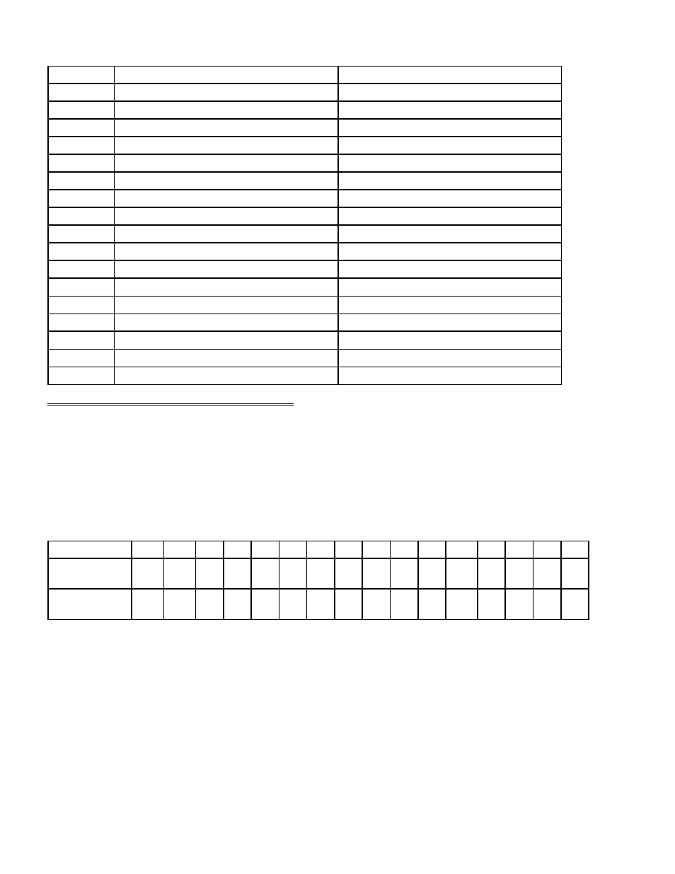
Table 5-2. DAS6402 I/O Map - ENHANCED Mode
(BOLD indicates register definition for DAS6402/16)
8254 Counter Control Register
None. No read back on 8254
BASE +15
CTR 2 Data - A/D Pacer Clock
CTR 2 Data - A/D Pacer Clock
BASE +14
CTR 1 Data - A/D Pacer Clock
CTR 1 Data - A/D Pacer Clock
BASE +13
CTR 0 Data: Preload for residual count
CTR 0 Data: (Residual/ End of acq)
BASE +12
UB,SEDIFF,MODE,Int source, ADGain
UB,SEDIFF,MODE,Int source, ADGain
BASE +11
DAC range, Pacer clock control
DAC range, Pacer clock control
BASE +10
Burst Enable, Interrupt, Pacer Source
Burst Enable, Interrupt, Pacer Source
BASE + 9
Extend modes and clear interrupts
FIFO, Interrupt Status, Clock rate
BASE + 8
D/A 1 Bits 4-11
None
BASE + 7
D/A 1 Bits 0-3
None
BASE + 6
D/A 0 Bits 4-11
None
BASE + 5
D/A 0 Bits 0-3
None
BASE + 4
Digital Output Bits 0-7
Digital Input bits 0-7 / External control
BASE + 3
32/64 Channel Mux (Word) /Reset FIFO
Post-Trigger Index Counter
BASE + 2
None
Do not use, use BASE only
BASE + 1
Software Start A/D Conversion
A/D bits 0(LSB) -15 (MSB) (Word)
BASE
Software Start A/D Conversion
A/D bits 0(LSB) -11 (MSB) (Word)
BASE
WRITE FUNCTION
READ FUNCTION
ADDRESS
5.2
A/D DATA WORD REGISTERS
In Enhanced Mode, two of the data registers are configured for 'Word' reads or writes, as opposed to performing the I/O operation
as separate byte reads or writes. These two registers are the A/D Data Register at the BASE+0, and the Channel Mux Hi/Lo
Register at BASE+2. Any IO accesses (reads or writes) to either of these registers is interpreted by the board as Word IO.
A/D DATA WORD REGISTER - 12 BIT
BASE + 0 Example, 300h, 768 Decimal
READ/WRITE
MA0
MA1
MA2
MA3
AD0
LSB
AD1
AD2
AD3
AD4
AD5
AD6
AD7
AD8
AD9
AD10
AD11
MSB
COMPATIBLE
0
0
0
0
AD0
LSB
AD1
AD2
AD3
AD4
AD5
AD6
AD7
AD8
AD9
AD10
AD11
MSB
ENHANCED
0
1
3
2
4
5
6
7
8
9
10
11
12
13
14
15
Mode
A read/write register. The A/D Data Register is configured as a word because REP INSW can be used to quickly read data from
the board, allowing for higher A/D conversion rates than would be possible if using DMA, which accesses the A/D data as two
bytes.
READ
On read, the 12-bit ADC value is presented in 'left-justified' format, with the most-significant ADC bit occupying the data word
bit position #15; the least-significant ADC bit occupies bit position #4 of the data word.
WRITE
A write to the base address will cause an A/D conversion, (Bits 0&1 of BASE+9 must be 0.)
ENHANCED MODE: The channel tag is not available in enhanced mode, thus the lowest four bits of the data word will be read
back as zero.
COMPATIBLE MODE: The channel tag is available in compatible mode, occupying the lowest four bits of the data word.
15