Crystals and resonators – Zilog Z8PE002 User Manual
Page 26

Z8PE002
Z8Plus OTP Microcontroller
ZiLOG
26
P R E L I M I N A R Y
DS008700-Z8X0799
OSCILLATOR OPERATION (Continued)
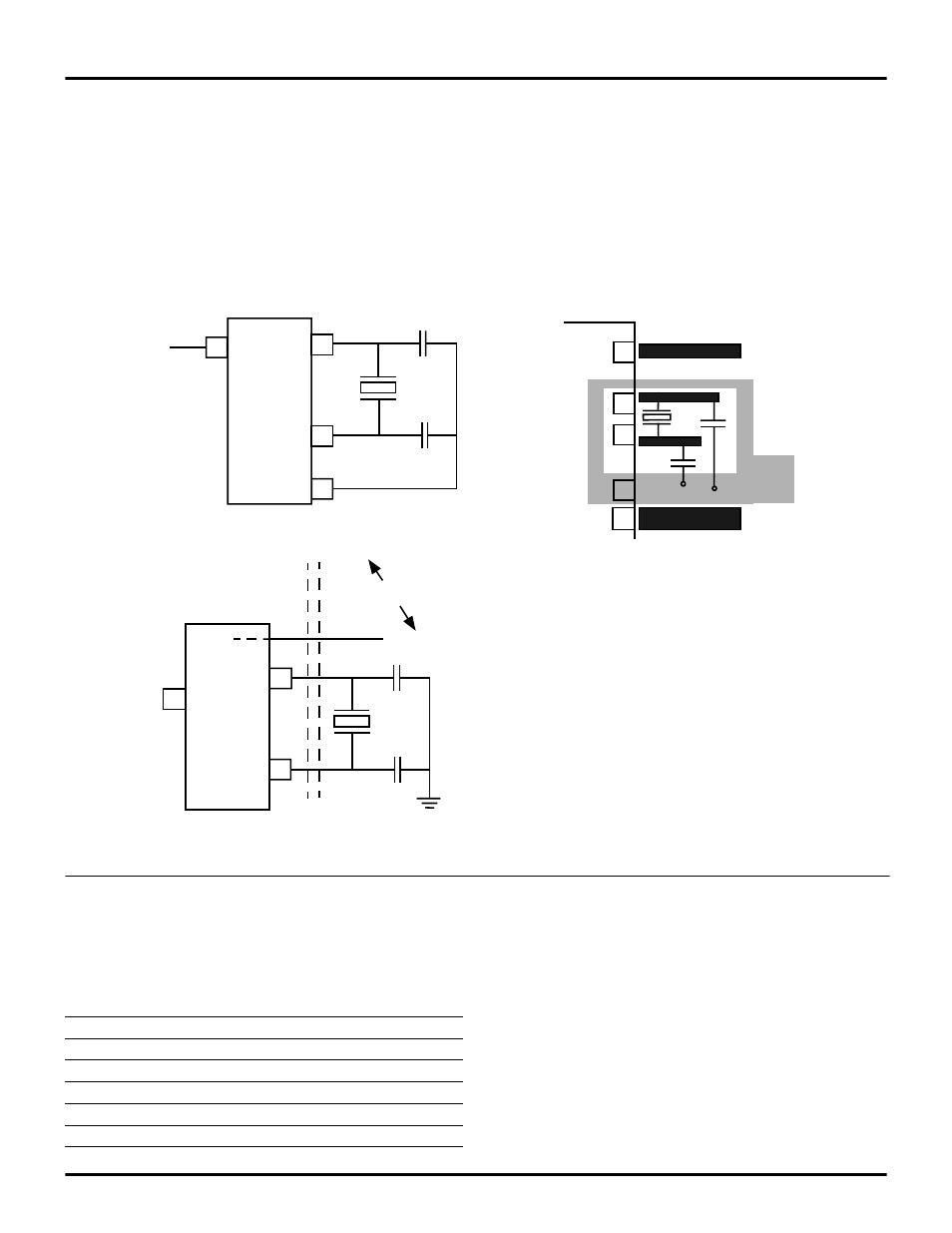
Circuit Board Design Rules
The following circuit board design rules are suggested:
•
To prevent induced noise, the crystal and load capaci-
tors should be physically located as close to the
Z8Plus as possible.
•
Signal lines should not run parallel to the clock oscil-
lator inputs. In particular, the crystal input circuitry
and the internal system clock output should be separat-
ed as much as possible.
•
V
CC
power lines should be separated from the clock
oscillator input circuitry.
•
Resistivity between
XTAL1
or
XTAL2
(and the other
pins) should be greater than 10 meg-Ohms.
Crystals and Resonators
Crystals and ceramic resonators (Figure 16) should exhibit
the following characteristics to ensure proper oscillation:
Depending on the operation frequency, the oscillator may
require additional capacitors,
C
1
and
C
2
, as illustrated in
Figure 16 and Figure 17. The capacitance values are de-
pendent on the manufacturer’s crystal specifications.
Figure 15. Circuit Board Design Rules
XTAL2
V
SS
XTAL1
Board Design Example
V
SS
Z8Plus
Z8Plus
Z8Plus
C
1
C
2
Clock Generator Circuit
Signals A B
Signal C
(Parallel traces
must be avoided)
(Top View)
17
16
15
17
16
XTAL1
XTAL2
X1
X2
PB0
V
CC
Crystal Cut
AT (crystal only)
Mode
Parallel, fundamental mode
Crystal Capacitance
<7pF
Load Capacitance
10pF < CL < 220 pF,
15 typical
Resistance
100 Ohms maximum
