Oscillator operation – Zilog Z8PE002 User Manual
Page 25

Z8PE002
ZiLOG
Z8Plus OTP Microcontroller
DS008700-Z8X0799
P R E L I M I N A R Y
25
OSCILLATOR OPERATION
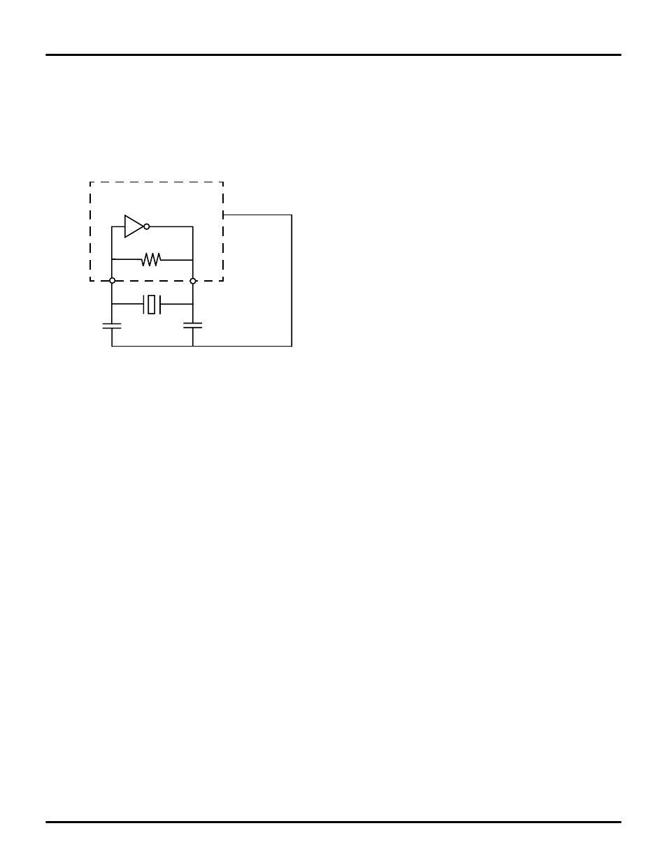
The Z8Plus MCU uses a Pierce oscillator with an internal
feedback resistor (Figure 14). The advantages of this circuit
are low-cost, large output signal, low-power level in the
crystal, stability with respect to
V
CC
and temperature, and
low impedances (not disturbed by stray effects).
One drawback to the Pierce oscillator is the requirement for
high gain in the amplifier to compensate for feedback path
losses. The oscillator amplifies its own noise at start-up until
it settles at the frequency that satisfies the gain/phase re-
quirements.
A x B = 1
; where
A = VO/VI
is the gain of the
amplifier, and
B = VI/VO
is the gain of the feedback element.
The total phase shift around the loop is forced to
0
(360 de-
grees).
V
IN
must be in phase with itself; therefore, the am-
plifier/inverter provides a 180-degree phase shift, and the
feedback element is forced to provide the other 180-degree
phase shift.
R1
is a resistive component placed from output to input of
the amplifier. The purpose of this feedback is to bias the am-
plifier in its linear region and provide the start-up transition.
Capacitor
C2
, combined with the amplifier output resis-
tance, provides a small phase shift. It also provides some
attenuation of overtones.
Capacitor
C
1
, combined with the crystal resistance, pro-
vides an additional phase shift.
Start-up time may be affected if
C
1
and
C
2
are increased dra-
matically in size. As
C
1
and
C
2
increase, the start-up time
increases until the oscillator reaches a point where it ceases
to operate.
For fast and reliable oscillator start-up over the manufac-
turing process range, the load capacitors should be sized as
low as possible without resulting in overtone operation.
Layout
Traces connecting crystal, caps, and the Z8Plus oscillator
pins should be as short and wide as possible to reduce par-
asitic inductance and resistance. The components (caps, the
crystal, and resistors) should be placed as close as possible
to the oscillator pins of the Z8Plus.
The traces from the oscillator pins of the integrated circuit
(IC) and the ground side of the lead caps should be guarded
from all other traces (clock,
V
CC
, address/data lines, and
system ground) to reduce cross talk and noise injection.
Guarding is usually accomplished by keeping other traces
and system ground trace planes away from the oscillator cir-
cuit, and by placing a Z8Plus device
V
SS
ground ring around
the traces/components. The ground side of the oscillator
lead caps should be connected to a single trace to the Z8Plus
device
V
SS
(GND)
pin. It should not be shared with any other
system-ground trace or components except at the Z8Plus
device
V
SS
pin. The objective is to prevent differential sys-
tem ground noise injection into the oscillator (Figure 15).
Indications of an Unreliable Design
There are two major indicators that are used in working de-
signs to determine their reliability over full lot and temper-
ature variations. They are:
Start-Up Time.
If start-up time is excessive, or varies
widely from unit to unit, there is probably a gain problem.
To fix the problem, the
C
1
and
C
2
capacitors require reduc-
tion. The amplifier gain is either not adequate at frequency,
or the crystal
R
’s are too large.
Output Level.
The signal at the amplifier output should
swing from ground to
V
CC
to indicate adequate gain in the
amplifier. As the oscillator starts up, the signal amplitude
grows until clipping occurs. At that point, the loop gain is
effectively reduced to unity, and constant oscillation is
achieved. A signal of less than 2.5 volts peak-to-peak is an
indication that low gain can be a problem. Either
C
1
or
C
2
should be made smaller, or a low-resistance crystal should
be used.
Figure 14. Pierce Oscillator with
Internal Feedback Circuit
XTAL2
Z8Plus
V
SS
XTAL1
C
1
C
2
R
I
V
1
A
V
0
