Clock, And its output is – Zilog Z8PE002 User Manual
Page 24
Z8PE002
Z8Plus OTP Microcontroller
ZiLOG
24
P R E L I M I N A R Y
DS008700-Z8X0799
CLOCK
The Z8Plus MCU derives its timing from on-board clock
circuitry connected to pins
XTAL1
and
XTAL2
. The clock
circuitry consists of an oscillator, a glitch filter, and a di-
vide-by-two shaping circuit. Figure 12 illustrates the clock
circuitry. The oscillator’s input is
XTAL1
and its output is
XTAL2
. The clock can be driven by a crystal, a ceramic res-
onator, LC clock, or an external clock source.
By selecting the
RC OSCILLATOR
option in the graphical
user interface (GUI), the circuit may instead be driven by
an external Resistor and Capacitor (
RC
13 illustrates this configuration. This design is limited to no
more than 4 MHz to restrict EMI noise.
Note: The reduced drive strength of this configuration also al-
lows the clock circuit to use a micropower-type crystal
(also known as a tuning fork) without reduction resis-
tors.
Figure 12. Clock Circuit
÷2
XTAL2
XTAL1
Glitch
Filter
÷4
÷8
WDT
Clock
Timer
Clock (TCLK)
Machine
Clock (SCLK)
(5 cycles
per in-
struction)
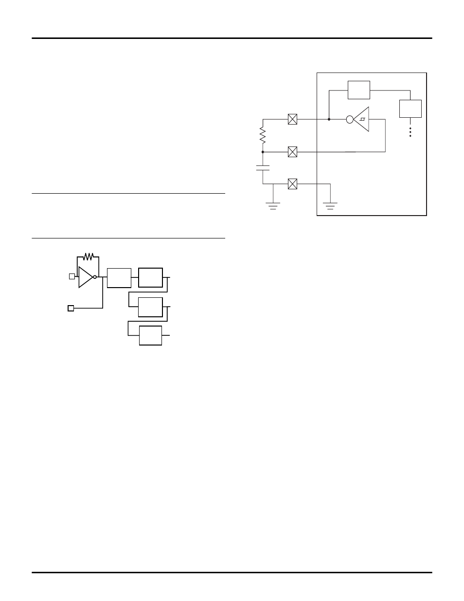
Figure 13. Z8Plus in RC Oscillator Mode
Glitch
Filter
SS
XTAL2
XTAL1
Note:
4 MHz max.
÷
2
R
C
V Pin