Power supply, Power supply –37 – Altera Transceiver Signal Integrity Development Kit, Stratix V GT Edition User Manual
Page 45
Chapter 2: Board Components
2–37
Power Supply
May 2014
Altera Corporation
Transceiver Signal Integrity Development Kit
Stratix V GT Edition Reference Manual
lists the flash memory component reference and manufacturing
information.
Power Supply
The development board’s power is provided through a laptop style DC power input.
The input voltage must be in the range of 14 V to 20 V. The DC voltage is then stepped
down to the various power rails used by the components on the board.
An on-board multi-channel power monitor device (LTC2978) measures both the
voltage and current for several specific board rails. This device has the capability to
trim voltage outputs ±10%.
F7
F_BSYN
1.8-V
AR7
Ready
B4
F_CEN
1.8-V
AP9
Chip enable
E6
F_CLK
1.8-V
AN6
Clock
F2
F_D0
1.8-V
AN11
Data bus
E2
F_D1
1.8-V
AM11
Data bus
G3
F_D2
1.8-V
AP12
Data bus
E4
F_D3
1.8-V
AN12
Data bus
E5
F_D4
1.8-V
AN10
Data bus
G5
F_D5
1.8-V
AM10
Data bus
G6
F_D6
1.8-V
AR11
Data bus
H7
F_D7
1.8-V
AR10
Data bus
E1
F_D8
1.8-V
AT12
Data bus
E3
F_D9
1.8-V
AU13
Data bus
F3
F_D10
1.8-V
AU12
Data bus
F4
F_D11
1.8-V
AU11
Data bus
F5
F_D12
1.8-V
AT11
Data bus
H5
F_D13
1.8-V
AW13
Data bus
G7
F_D14
1.8-V
AV13
Data bus
E7
F_D15
1.8-V
AW11
Data bus
F8
F_OEN
1.8-V
AN9
Output enable
D4
F_RSTN
1.8-V
AL8
Reset
G8
F_WEN
1.8-V
AM8
Write enable
C6
F_WPN
1.8-V
AP6
Write protect
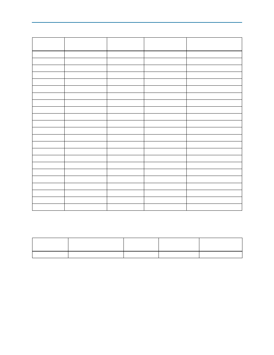
Table 2–37. Flash Pin Assignments, Schematic Signal Names, and Functions (Part 2 of 2)
Board
Reference (U21)
Schematic Signal
Name
I/O Standard
Stratix V GT Device
Pin Number
Description
Table 2–38. Flash Memory Component Reference and Manufacturing Information
Board Reference
Description
Manufacturer
Manufacturing
Part Number
Manufacturer
Website
U21
1-Gb synchronous flash
Micron
PC28F00AP30BF