Max ii cpld system controller, Max ii cpld system controller –9 – Altera Transceiver Signal Integrity Development Kit, Stratix V GT Edition User Manual
Page 17
Chapter 2: Board Components
2–9
MAX II CPLD System Controller
May 2014
Altera Corporation
Transceiver Signal Integrity Development Kit
Stratix V GT Edition Reference Manual
MAX II CPLD System Controller
The board utilizes the EPM2210F256C3N System Controller, an Altera MAX II CPLD,
for the following purposes:
■
FPGA configuration from flash memory
■
Temperature monitoring
■
Fan control
■
Virtual JTAG interface for PC-based power and temperature GUI
■
Control registers for clocks
■
Control registers for remote system update
■
Register with CPLD design revision and board information (read-only)
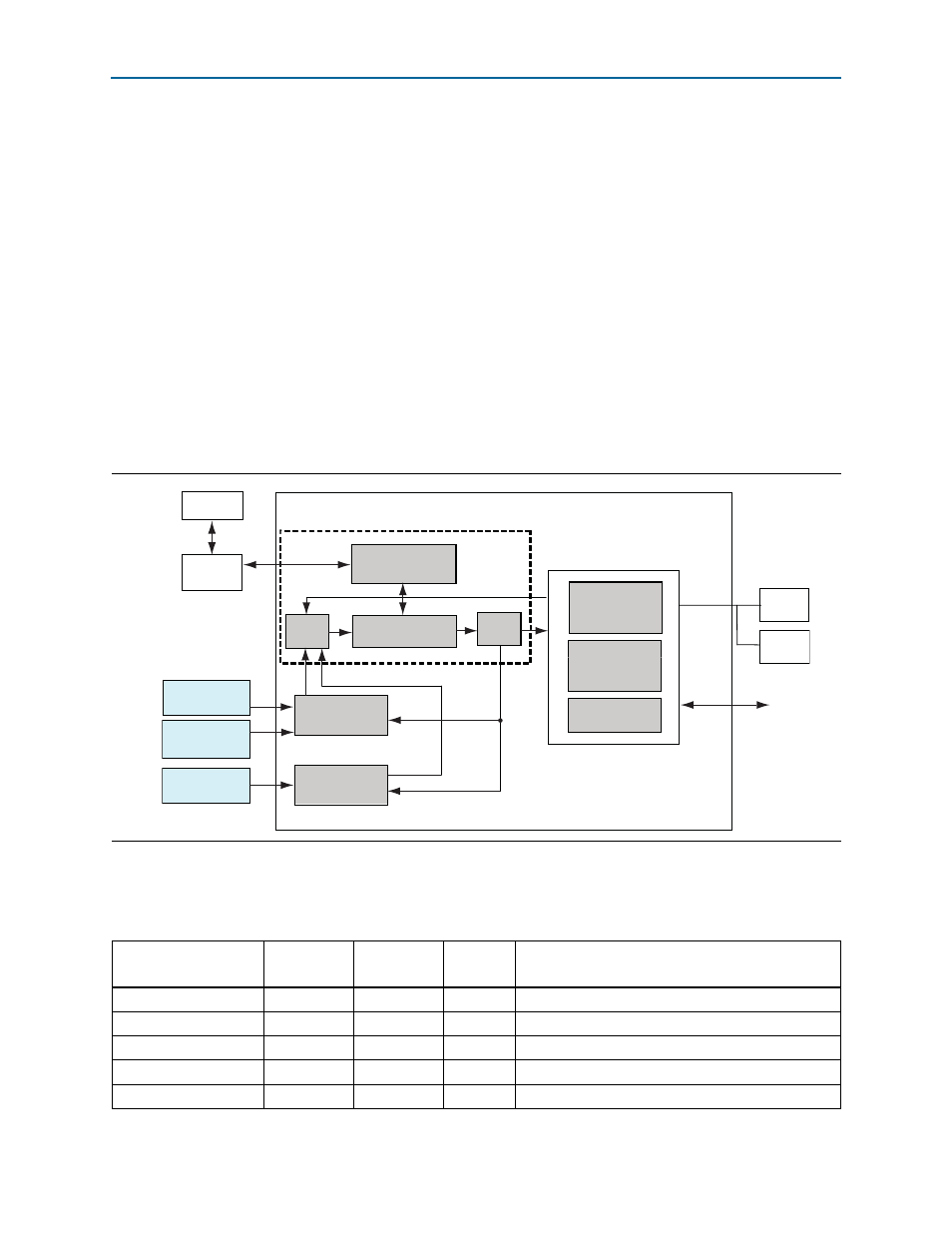
illustrates the MAX II CPLD System Controller's functionality and external
circuit connections as a block diagram.
lists the I/O signals present on the MAX II CPLD System Controller. The
signal names and functions are relative to the MAX II device (U19).
Figure 2–2. MAX II CPLD System Controller Block Diagram
MAX1619
Controller
Information
Register
Embedded
USB-Blaster
MAX II CPLD
SLD-HUB
PFL
FSD Bus
Temperature
Measure Results
Virtual-JTAG
PC
S5_VCCA
Measure Results
FPGA
LTC2978
Controller
Flash
GPIO
Decoder
Encoder
JTAG Control
Control
Register
Power Monitor
Table 2–5. MAX II CPLD System Controller Device Pin-Out (Part 1 of 5)
Schematic Signal
Name
MAX II CPLD
Pin Number
Stratix V GT
Pin Number
I/O
Standard
Description
50MHZ_MAXLL_CLK
H5
—
2.5-V
50 MHz clock input
ALERTn
D2
E8
2.5-V
Temperature monitor alert
CONF_DONE
T13
AB12
2.5-V
Configuration done
CONFIG_D0
T11
AR33
2.5-V
Configuration data
CONFIG_D1
T10
AU32
2.5-V
Configuration data