Featured device: stratix v gt fpga, I/o resources, Featured device: stratix v gt fpga –6 – Altera Transceiver Signal Integrity Development Kit, Stratix V GT Edition User Manual
Page 14: I/o resources –6
2–6
Chapter 2: Board Components
Featured Device: Stratix V GT FPGA
Transceiver Signal Integrity Development Kit
May 2014
Altera Corporation
Stratix V GT Edition Reference Manual
Featured Device: Stratix V GT FPGA
The development board features the Stratix V GT 5SGTMC7K2F40C2 device (U29) in
a 1517-pin FineLine BGA package.
f
For more information about the Stratix V device family, refer to
describes the features of the Stratix V GT 5SGTMC7K2F40C2 device.
lists the Stratix V GT component reference and manufacturing information.
I/O Resources
summarizes the FPGA I/O usage by function on the Stratix V GT
transceiver signal integrity development board.
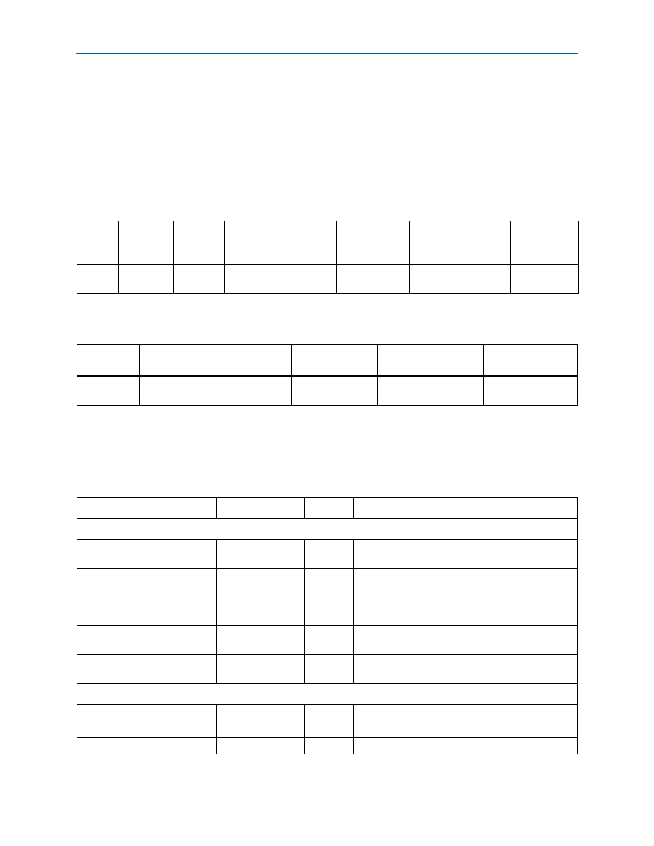
Table 2–2. Stratix V GT Device Features
ALMs
Equivalent
LEs
Registers
M20K
Blocks
MLAB
Blocks (Mb)
18-bit × 18-bit
Multipliers
PLLs
Transceiver
Channels
(12.5 Gbps)
Package Type
234,720
622,000
939,000
2,560
7.16
512
28
36
1517-pin
FineLine BGA
Table 2–3. Stratix V GT Component Reference and Manufacturing Information
Board
Reference
Description
Manufacturer
Manufacturing
Part Number
Manufacturer
Website
U29
FPGA, Stratix V GT F1517, 622K
LEs, lead-free
Altera
Corporation
5SGTMC7K2F40C2
Table 2–4. Stratix V GT I/O Usage Summary (Part 1 of 3)
Function
I/O Type
I/O Count
Description
FPGA Transceiver Clocks
Programmable differential clock
LVDS input
4
Differential REFCLK input to feed the even-numbered
channels on the left side of the Stratix V GT device.
Programmable differential clock
LVDS input
4
Differential REFCLK input to feed the odd-numbered
channels on the left side of the Stratix V GT device.
Programmable differential clock
LVDS input
4
Differential REFCLK input to feed the even-numbered
channels on the right side of the Stratix V GT device.
Programmable differential clock
LVDS input
4
Differential REFCLK input to feed the odd-numbered
channels on the right side of the Stratix V GT device.
External differential clock inputs
LVDS input
4 pairs
Differential REFCLK input for one SMA pair per clock
buffer.
FPGA Global Clocks
50-MHz clock
2.5-V CMOS input
1
Global clock input.
Spread Spectrum clock
2.5-V CMOS input
2
Differential global clock.
SMA differential clock input
LVDS input
2
Differential global clock.