Altera Transceiver Signal Integrity Development Kit, Stratix V GT Edition User Manual
Page 11
Chapter 2: Board Components
2–3
Board Overview
May 2014
Altera Corporation
Transceiver Signal Integrity Development Kit
Stratix V GT Edition Reference Manual
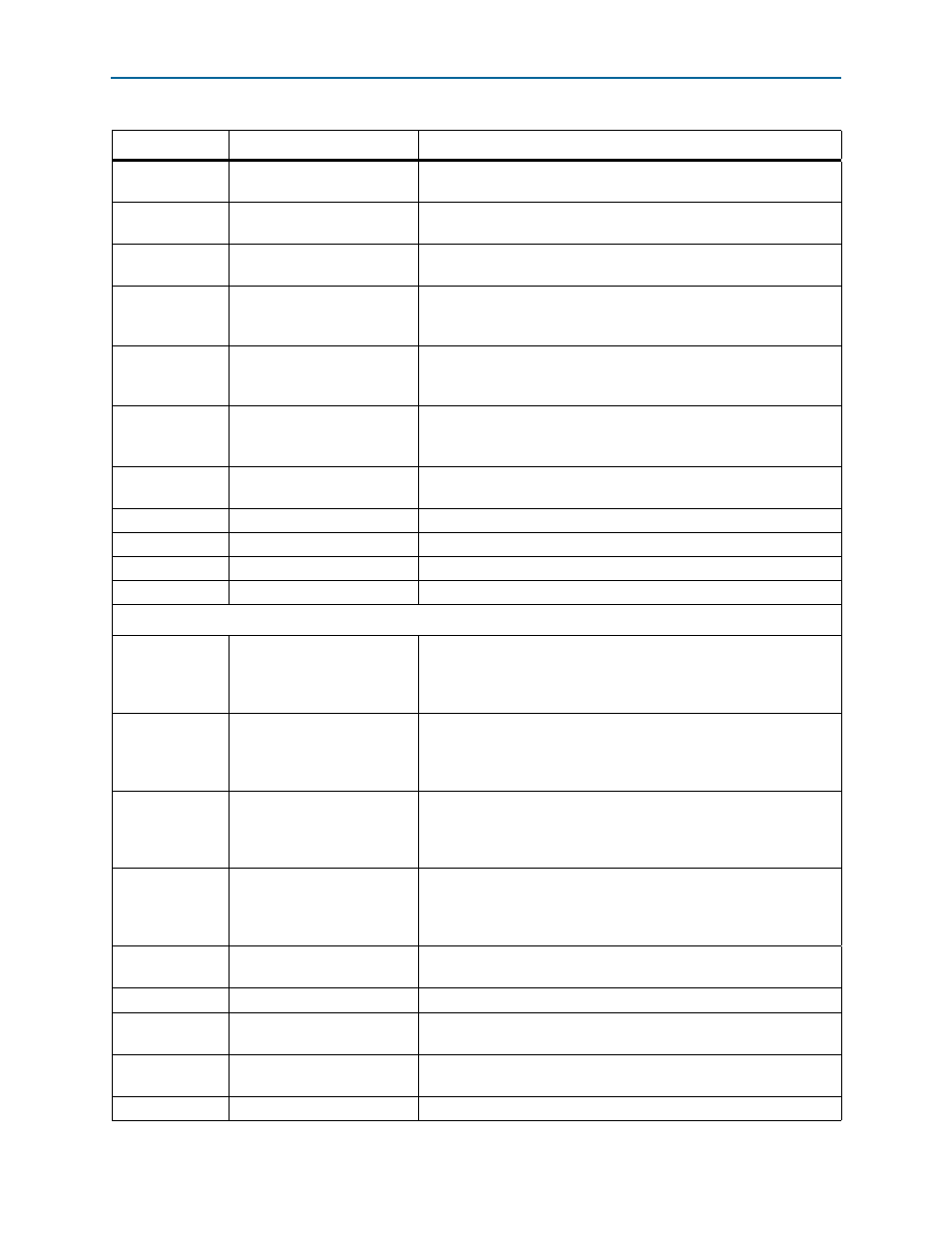
J28
Program select jumper
Toggles the program LEDs to select which FPGA image to load on
power-up; 0 selects factory image and 1 selects user-defined image.
S7
FPP configuration/MAX II
bypass DIP switch
Select the configuration mode from the MAX II CPLD.
SW5
Spread spectrum clock
settings DIP switch
Sets the spread spectrum output clock frequency and down-spread
percentages.
SW2 (pin2-7)
VCCA_GXB voltage selection
jumper
Selects V
CCA
voltage to the FPGA. When the jumper is set to close
position, the V
CCA
voltage is 3.0 V (default). When set to open position,
the V
CCA
voltage is 2.5 V.
SW2 (pin 1-8)
VCCRT voltage selection
jumper
Selects V
CCRT
voltage to the FPGA. When the jumper is set to close
position, the V
CCRT
voltage is 1.0 V (default). When set to open position,
the V
CCRT
voltage is 0.85 V.
J26
Fan control jumper
Selects whether the fan is always on or the FPGA automatically
controls the fan. To set it to its default setting of always on, connect
jumper pin 2-3. Connect jumper pin 1-2 to set the fan in auto mode.
D7
Fan LED
Indicates an over-temperature condition in the FPGA and a fan should
be attached to the FPGA and running.
D8
Load LED
Illuminates during embedded USB-Blaster data transfers.
D9
Error LED
Illuminates when the FPGA configuration from flash fails.
D3
Power LED
Illuminates when 14-V power is present.
D12-D17
Ethernet LEDs
Indicates the connection speed as well as transmit or receive activity.
Clock Circuitry
Y3
Programmable oscillator
Feeds even-numbered REFCLKs on left side of the Stratix V GT device
and trigger an output at board reference J81. The external input is
available at board reference J79 and J80. The default frequency is
644.53125 MHz.
Y4
Programmable oscillator
Feeds odd-numbered REFCLKs on left side of the Stratix V GT device
and trigger an output at board reference J85. The external input is
available at board reference J83 and J84. The default frequency is
706.25 MHz.
Y5
Programmable oscillator
Feeds even-numbered REFCLKs on right side of the Stratix V GT device
and trigger an output at board reference J88. The external input is
available at board reference J86 and J87. The default frequency is
625 MHz.
Y6
Programmable oscillator
Feeds odd-numbered REFCLKs on right side of the Stratix V GT device
and trigger an output at board reference J91. The external input is
available at board reference J89 and J90. The default frequency is
875 MHz.
SW6
Transceiver clock input select
DIP switch
Selects the SMA or oscillator as the clock input.
Y2
50-MHz oscillator
50.000-MHz crystal oscillator for general purpose logic.
X3
25/100/125/200-MHz core
clock selectable oscillator
Selects the core clock frequency. The default frequency is 100 MHz.
SW5
Spread spectrum selection
switch
Select either the core or spread spectrum clock. Pin 1-2 selects S0 and
S1 while pin 3-4 selects SS0 and SS1.
J70 and J71
External core clock input
SMA external input at CLK10 p/n.
Table 2–1. Transceiver Signal Integrity Development Kit Components (Part 2 of 4)
Board Reference
Type
Description