Ii processor, Figure 2–4. max ii and flash fpp configuration – Altera Transceiver Signal Integrity Development Kit, Stratix V GT Edition User Manual
Page 24
2–16
Chapter 2: Board Components
Configuration, Status, and Setup Elements
Transceiver Signal Integrity Development Kit
May 2014
Altera Corporation
Stratix V GT Edition Reference Manual
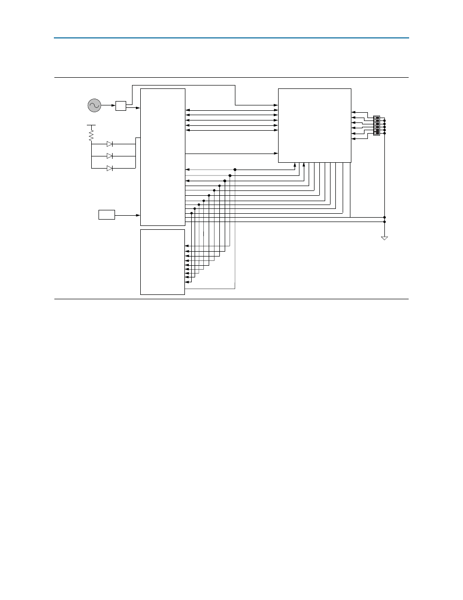
shows the MAX II and flash FPP configuration.
f
For more information on the flash memory map storage, re
.
Flash Programming
Flash programming is possible through a variety of methods using the Stratix V GT
device.
The first method is to use the factory design called the Board Update Portal. This
design is an embedded webserver, which serves the Board Update Portal web page.
The web page allows you to select new FPGA designs including hardware, software,
or both in an industry-standard S-Record File (.flash) and write the design to the user
hardware page (page 1) of the flash over the network.
The secondary method is to use the pre-built PFL design included in the development
kit. The development board implements the Altera PFL megafunction for flash
programming. The PFL megafunction is a block of logic that is programmed into an
Altera programmable logic device (FPGA or CPLD). The PFL functions as a utility for
writing to a compatible flash device. This pre-built design contains the PFL
megafunction that allows you to write either page 0, page 1, or other areas of flash
over the USB interface using the Quartus II software. This method is used to restore
the development board to its factory default settings.
Other methods to program the flash can be used as well, including the Nios
®
II
processor.
Figure 2–4. MAX II and Flash FPP Configuration
MAX II CPLD
System Controller
CONF_D[15:0]
DCLK
DCLK
CLKxP
F_AD[26:1]
F_D[15:0]
D[15:0]
nSTATUS
nCONFIG
CONF_DONE
MSEL0
MSEL1
MSEL2
MSEL3
nCE
CFI Flash
Green LED (Factory Image)
Green LED (User Image)
Red LED (Error Image)
F_CEn
F_OEn
F_WEn
DEV_CLRn
nCONFIG
CONF_DONE
FSM Bus Interface
PGMSEL
PGM [2:0]
CLKBUF
nSTATUS
CLK
ADVn
CONFIG_ERR,
FACTORY_IMAGE,
USER_IMAGE LEDs
2.5 V
F_CLK
F_RSTn
RESETn
RY/BYn
WPn
RY/BYn
WPn
50 MHz
MSEL4
MAX_BYPASS
DIP Switch
(S7)
RESETn
F_AD[26:1]
F_D[15:0]
F_CEn
F_OEn
F_WEn
ADVn
F_CLK
Stratix V GT
FPGA