Hardware requirements, Hardware requirements -3 – Altera Transceiver SI User Manual
Page 11

Altera Corporation
Getting Started User Guide
2–3
June 2006
Transceiver Signal Integrity Development Kit, Stratix II GX Edition
Getting Started
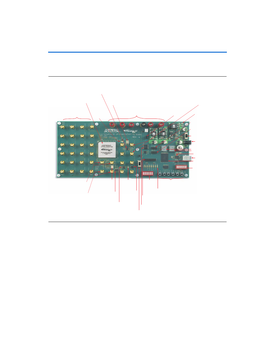
Figure 2–1
shows the Stratix II GX EP2SGX90 transceiver signal integrity
development board.
Figure 2–1. Stratix II GX Transceiver Signal Integrity Development Board
f
Refer to the Stratix II GX EP2SGX90 Transceiver Signal Integrity
Development Board Reference Manual (available on the Transceiver SI
Development Kit, Stratix II GX Edition CD-ROM) for information on the
board’s components.
Hardware Requirements
All of the hardware that you need to use the board is provided with the
Transceiver Signal Integrity Development Kit, Stratix II GX Edition.
Clock
Setting
DIP S
w
itch
Bank (S
8
)
User DIP S
w
itch
Bank (S7)
User P
u
sh-B
u
tton
S
w
itches (S1 thro
u
gh S6)
Stratix II GX De
v
ice (U20)
D
u
al 7-Segment
Displays (D9, D10)
Po
w
er S
w
itch (S10)
User LEDs
(D1 thro
u
gh D
8
)
Slide
S
w
itch (S9)
De
bu
g
Header (J1)
Clock
Generator (U5)
Differential
Fan-o
u
t
B
u
ffer (U
8
)
Differential to
Single-Ended
B
u
ffer (U7)
156.25-MHz
Oscillator (U9)
25-MHz
Crystal (U6)
EPCS64 De
v
ice (U22)
16 M
b
ytes Flash
Memory (U19)
USB Connector (J2)
USB Interface (U2)
Temperat
u
re Sensor
w
ith Alarm (U17)
SMA Transmit &
Recei
v
e Connectors
(J26 thro
u
gh J49)
Po
w
er S
u
pply Inp
u
t
10-pin Config
u
ration Header
for EPCS64 De
v
ice (J23)
10-pin JTAG Config
u
ration
Header for FPGA (J24)
Config
u
ration
Done LED (D14)
Optional Po
w
er Inp
u
t
Connection Jacks (J15, J17-21)
J
u
mper Header for
V
CCH
V
oltage (J50)
SMA Inp
u
t Clock
Connectors for FPGA (J12, J14)
SMA O
u
tp
u
t Clock Connectors
Reference Clock for Q
u
ad 1
Transcei
v
ers (J7, J
8
)
SMA O
u
tp
u
t Clock Connectors
Reference Clock for Q
u
ad 3
Transcei
v
ers (J9, J10)
50-MHz Oscillator
Used for System Clock (U10)
Po
w
er LED (D13)
