Pll worksheet, Pll worksheet -26 – Altera PowerPlay Early Power Estimator User Manual
Page 36
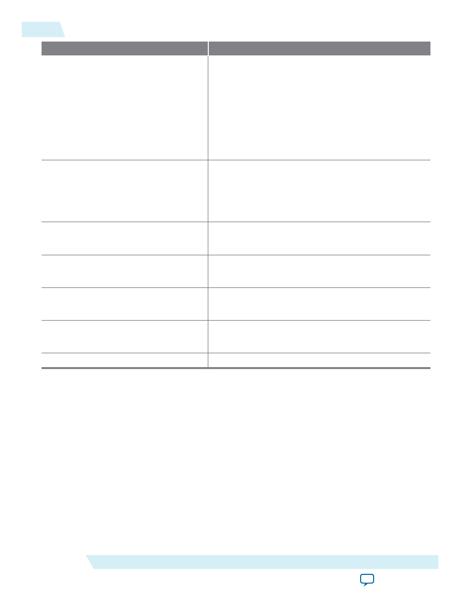
Column Heading
Description
Thermal Power (W)–Routing
This shows the power dissipation due to estimated routing
(in watts).
Routing power depends on placement-and-routing
information, which is a function of design complexity. The
values shown represent the routing power based on
experimentation of more than 100 designs.
For detailed analysis based on your design’s routing, use the
Quartus II PowerPlay Power Analyzer. This value is
automatically calculated.
Thermal Power (W)–Block
This shows the power dissipation due to internal and load
toggling of the I/O (in watts).
For accurate analysis based on your design’s exact I/O
configuration, use the Quartus II PowerPlay Power
Analyzer. This value is automatically calculated.
Thermal Power (W)–Total
This shows the total power dissipation (in watts). The total
power dissipation is the sum of the routing and block
power. This value is automatically calculated.
Supply Current (A)–I
CC
This shows the current drawn from the V
CC
power rail and
powers the internal digital circuitry. This value is automati‐
cally calculated.
Supply Current (A)–I
CCPD
This shows the current drawn from the V
CCPD
power rail
and powers the pre-drive circuitry. This value is automati‐
cally calculated.
Supply Current (A)–I
CCIO
This shows the current drawn from the V
CCIO
power rail.
Some of this current may be drawn into off-chip termina‐
tion resistors. This value is automatically calculated.
User Comments
Enter any comments. This is an optional entry.
For more information about the I/O standard termination scheme of the supported device families, refer
to the “I/O Features” chapter of the respective device handbook.
PLL Worksheet
Altera FPGA devices feature PLLs for general use. Each row in the PLL worksheet of the PowerPlay EPE
spreadsheet represents one or more PLLs in the device. Enter the maximum output frequency and the
VCO frequency for each PLL. You must also specify whether each PLL is an LVDS, fractional, left/right,
or top/bottom PLL.
When a PLL drives source synchronous SERDES hardware, it is referred to as an LVDS PLL. If you are
using dedicated transmitters or receivers and are using an LVDS PLL to implement serialization or
deserialization, specify an LVDS PLL and enter the power information in the PLL worksheet. LVDS PLLs
drive LVDS clock trees and dynamic phase alignment (DPA) buses at the voltage-controlled oscillator
(VCO) frequency. If an LVDS PLL drives the LVDS hardware only, enter the appropriate VCO frequency
and specify an output frequency of 0 MHz. If the LVDS PLL also drives a clock to a pin or to the core,
specify that clock frequency as the output frequency.
3-26
PLL Worksheet
UG-01070
2015.01.20
Altera Corporation
PowerPlay Early Power Estimator Worksheets