Altera PowerPlay Early Power Estimator User Manual
Page 32
3–18
Altera
Corporation
PowerPlay Early Power Estimator For Arria GX FPGAs
May 2008
PowerPlay Early Power Estimator Inputs
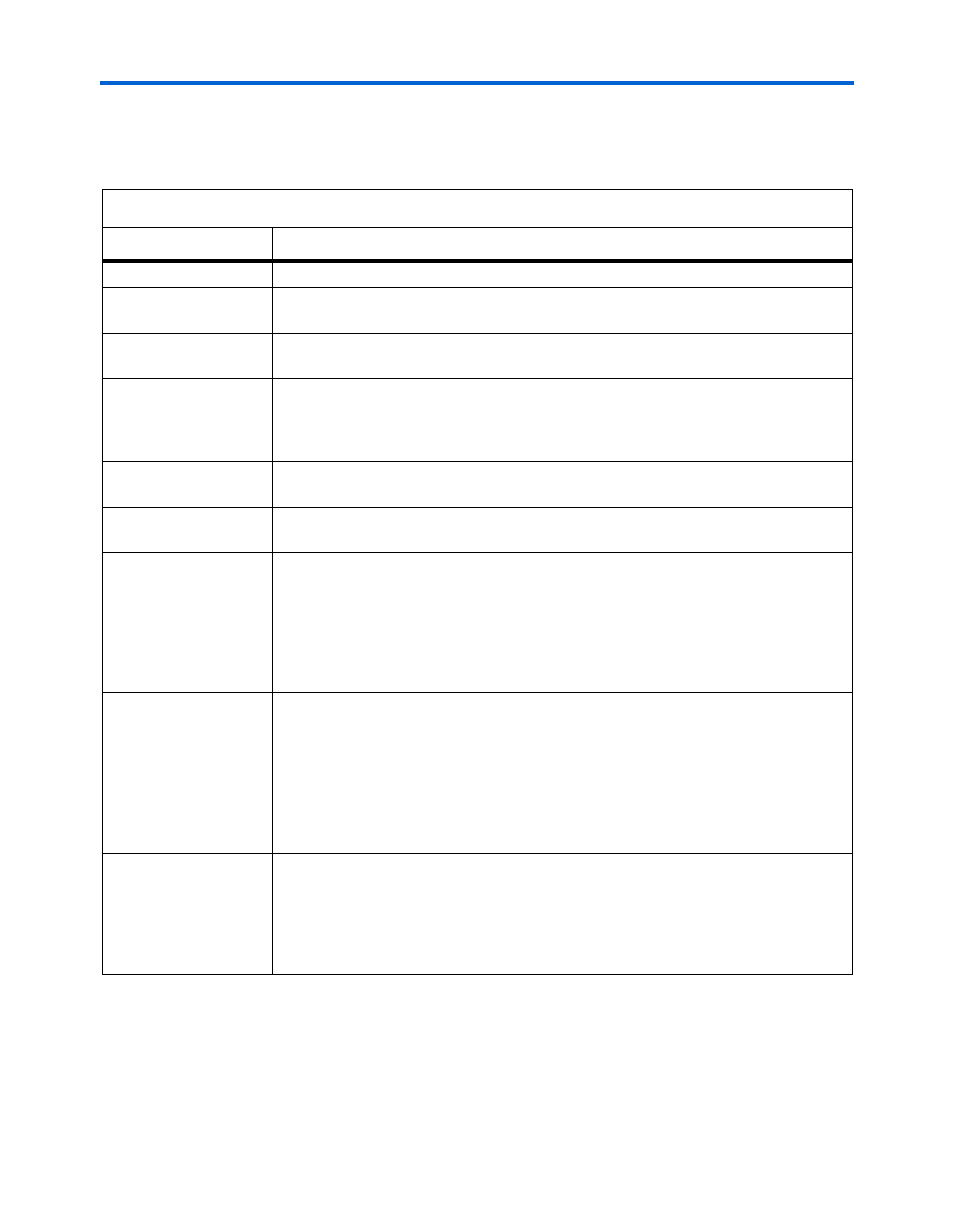
Table 3–6
describes the I/O module parameters in the I/O section of the
PowerPlay Early Power Estimator.
Table 3–6. I/O Module Information in the I/O Section (Part 1 of 2)
Column Heading
Description
Module
Enter a name for the module in this column. This is an optional value.
I/O Standard
Select the I/O standard used for the input, output or bidirectional pins in this module
from the list. The calculated I/O power varies based on the I/O standard.
Drive Strength/ On-chip
Termination
Select the drive strength or on-chip termination implemented for the I/O pin(s) in this
module. Drive strength and on-chip termination are mutually exclusive.
Clock Freq (MHz)
Enter the clock frequency (in MHz).
100 MHz with a 12.5% toggle means that each I/O pin toggles 12.5 million times per
second (100 × 12.5%).
# Output Pins
Enter the number of output pins used in this module. A differential pair of pins should
be considered as one pin.
# Input Pins
Enter the number of input pins used in this module. A differential pair of pins should be
considered as one pin.
# Bidir Pins
Enter the number of bidirectional pins used in this module. The I/O pin is treated as an
output when its output enable signal is active and an input when the output enable is
disabled.
An I/O configured as bidirectional but used only as an output consumes more power
than one configured as an output-only, due to the toggling of the input buffer every time
the output buffer toggles (they share a common pin).
I/O Bank
Select the I/O bank that the module is located in. If you do not know which I/O bank
the pins are assigned to, leave the value as “?.” Assigning the I/O module to a bank
checks whether or not your I/O voltage assignments are compatible. This allows
per-bank I
CCIO
reporting.
The PowerPlay Early Power Estimator spreadsheet does not take any I/O placement
constraints into consideration except if the I/O bank, I/O standard, I/O voltage are
compatible.
Toggle %
Enter the average percentage of output and bidirectional pins toggling on each clock
cycle. The toggle percentage ranges from 0 to 200%. If the pin uses a double data rate
(DDR), you can set the data rate to single data rate (SDR) and double the toggle
percentage. The Quartus II software often uses this method to output information.
Typically the toggle percentage is 12.5%. To be more conservative, you can use a
higher toggle percentage.