The flash tab, Read, The flash tab –8 – Altera Arria V GX FPGA User Manual
Page 30: Read –8
6–8
Chapter 6: Board Test System
Using the Board Test System
Arria V GX FPGA Development Kit
July 2012
Altera Corporation
User Guide
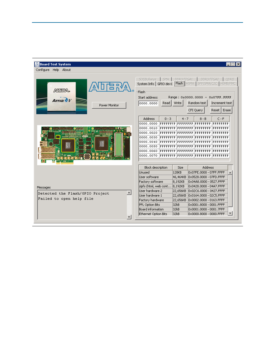
The Flash Tab
The Flash tab (
) allows you to read and write flash memory on your board.
The following sections describe the controls on the Flash tab.
Read
The Read control reads the flash memory on your board. To see the flash memory
contents, type a starting address in the text box and click Read. Values starting at the
specified address appear in the table. The flash memory addresses display in the
format the Nios II processor within the FPGA uses, that is, each flash memory address
is offset by 0x0800.0000. Valid are entries are 0x0000.0000 through 0x07FF.FFFF.
1
If you enter an address outside of the flash memory address space, a warning
message identifies the valid flash memory address range.
Figure 6–4. The Flash Tab