Factory default switch and jumper settings, Factory default switch and jumper settings –2, Figure 4–1 – Altera Arria V GX FPGA User Manual
Page 16: Figure 4–2
4–2
Chapter 4: Development Board Setup
Factory Default Switch and Jumper Settings
Arria V GX FPGA Development Kit
July 2012
Altera Corporation
User Guide
Factory Default Switch and Jumper Settings
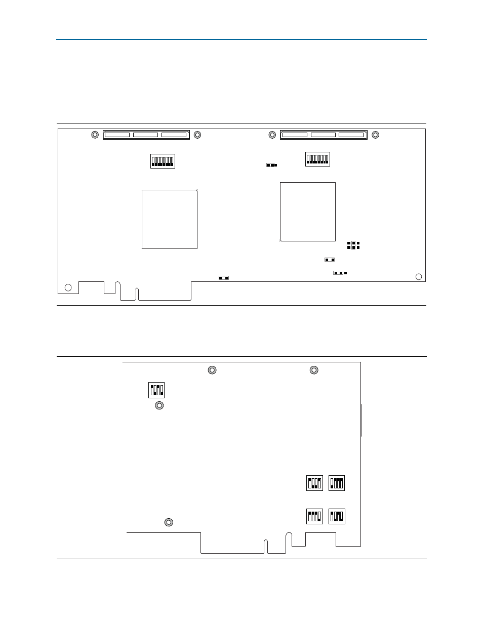
This section shows the factory switch and jumper settings for the Arria V GX FPGA
development board.
shows the switch and jumper locations and the
default position of each switch and jumper on the top side of the board.
shows the switch locations and the default position of each switch on the
bottom side of the board.
Figure 4–1. Switch Locations and Default Settings on the Board Top
J23
J28
SW3
(installed)
FAN1
J14
(installed)
FAN2
J5
7
2.5V
FMC_VCCPD
3.3V
6543210
SW2
76543210
USER_DIP1
USER_DIP2
ON
ON
J11
1.8V 2.5V 3.3V
Figure 4–2. Switch Locations and Default Settings on the Board Bottom
SW4
SW8
4
2
1
ON
MSEL2
4
2
1
MSEL 1
PCIe Width
SW5
ON
1 2 3 4
Factory2
Factory1
CLK_EN
CLK_SEL
HSMA
HSMB
FMC
SW6
JTAG_CHAIN
ON
1 2 3 4
SW7
ON
1 2 3 4
1 2 3 4
ON
3
3