Altera Arria V GX FPGA User Manual
Page 18
4–4
Chapter 4: Development Board Setup
Factory Default Switch and Jumper Settings
Arria V GX FPGA Development Kit
July 2012
Altera Corporation
User Guide
3. Set DIP switch bank (SW6) to match
4. Set DIP switch bank (SW7) to match
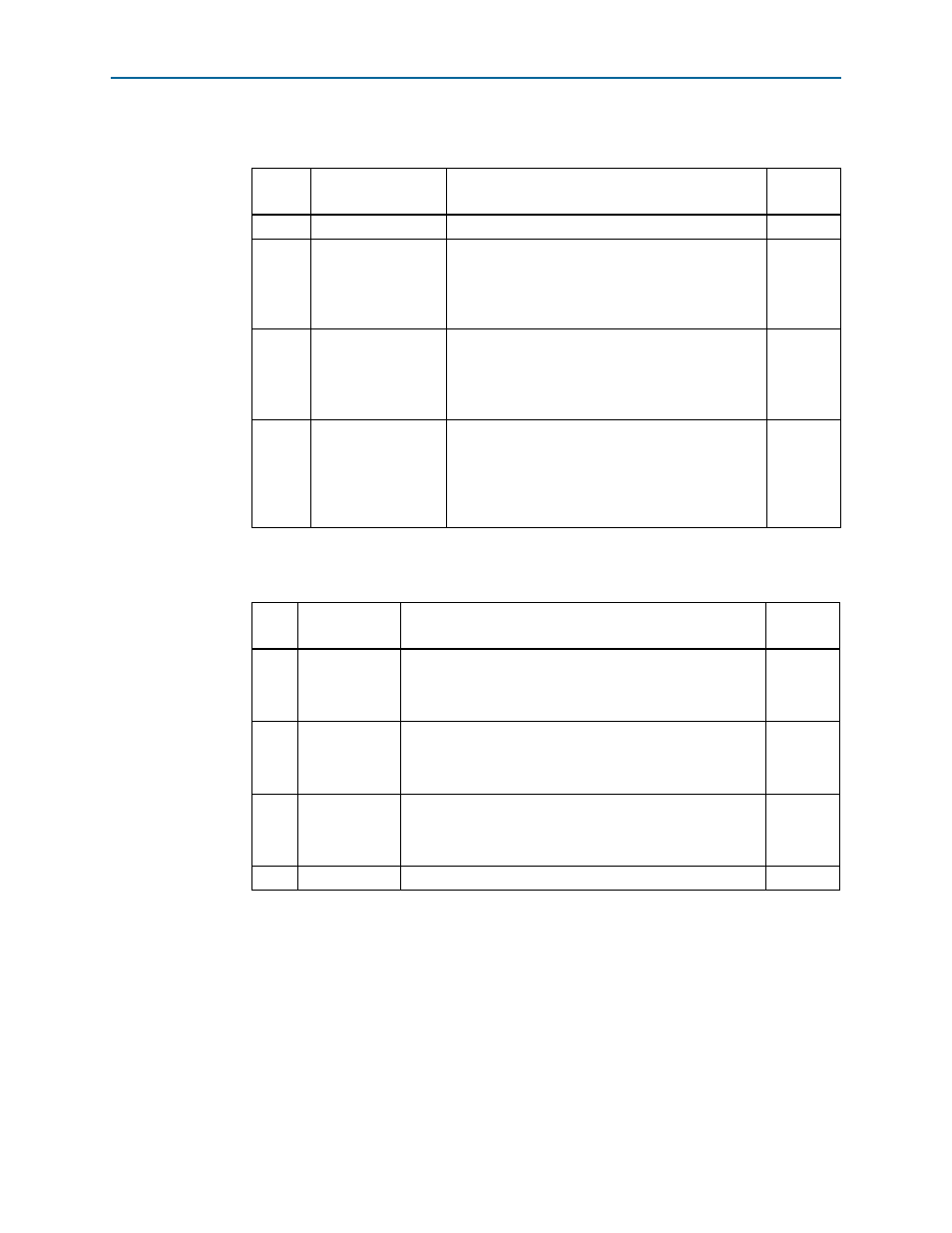
Table 4–3. SW6 JTAG Dip Switch Settings
Switch
Board
Label
Function
Default
Position
1
—
—
OFF
2
HSMA_JTAG_EN
Switch 2 has the following options:
■
ON, (logical 0) = HCMC Port A not in JTAG chain.
■
OFF, (logical 1) = Include HCMC Port A in the
JTAG chain.
ON
3
HSMB_JTAG_EN
Switch 3 has the following options:
■
ON, (logical 0) = HCMC Port B not in JTAG chain.
■
OFF, (logical 1) = Include HCMC Port B in the
JTAG chain.
ON
4
FMC_JTAG_EN
Switch 4 has the following options:
■
ON, (logical 0) = FMC connector not in JTAG
chain.
■
OFF, (logical 1) = Include FMC connector in the
JTAG chain.
ON
Table 4–4. SW7 PCIe DIP Switch Settings
Switc
h
Board
Label
Function
Default
Position
1
PCIE_PRSNT2
n_x1
Switch 1 has the following options:
■
ON (0) = x1 presence detect is enabled.
■
OFF (1) = x1 presence detect is disabled.
ON
2
PCIE_PRSNT2
n_x4
Switch 2 has the following options:
■
ON (0) = x4 presence detect is enabled.
■
OFF (1) = x4 presence detect is disabled.
ON
3
PCIE_PRSNT2
n_x8
Switch 3 has the following options:
■
ON (0) = x8 presence detect is enabled.
■
OFF (1) = x8 presence detect is disabled.
ON
4
—
—
OFF