Altera Arria V GT FPGA User Manual
Page 17
Chapter 4: Development Board Setup
4–3
Factory Default Switch and Jumper Settings
November 2012
Altera Corporation
Arria V GT FPGA Development Kit
User Guide
To restore the switches to their factory default settings, perform the following steps:
1. Set DIP switch bank (SW4) to match
2. Set DIP switch bank (SW5) to match
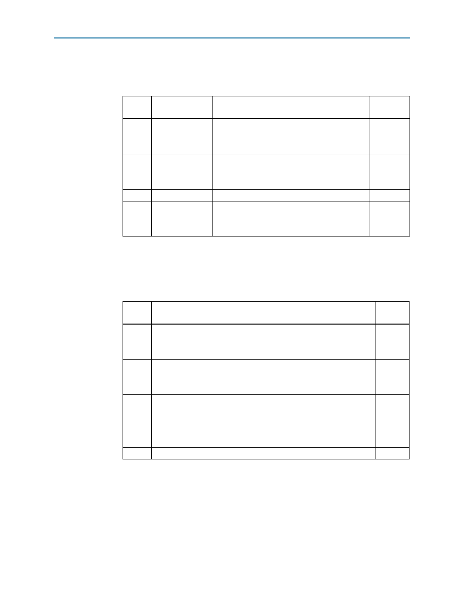
Table 4–1. SW4 FPGA2 MSEL Dip Switch Settings
Switch
Board
Label
Function
Default
Position
1
FPGA2_MSEL[1]
Switch 1 has the following options:
■
When ON, a logic 0 is selected.
■
When OFF, a logic 1 is selected.
ON
2
FPGA2_MSEL[2]
Switch 2 has the following options:
■
When ON, a logic 0 is selected.
■
When OFF, a logic 1 is selected.
OFF
3
—
—
ON
4
FPGA2_MSEL[4]
Switch 4 has the following options:
■
When ON, a logic 0 is selected.
■
When OFF, a logic 1 is selected.
OFF
(1) Ensure that all MSEL setting are in a defined configuration scheme as shown in
e Arria V Device Handbook.
Table 4–2. SW5 Board Settings Dip Switch
Switch
Board
Label
Function
Default
Position
1
CLK_SEL
Switch 1 has the following options:
■
ON, (logical 0) = SMA input clock select.
■
OFF, (logical 1) = programmable oscillator clock select.
OFF
2
CLK_EN
Switch 2 has the following options:
■
ON, (logical 0) = on-board oscillator disable.
■
OFF, (logical 1) = on-board oscillator enable.
ON
3
Factory1
Switch 3 has the following options:
■
ON, (logical 0) = load the factory design for Arria V
FPGA 1 from flash at power up.
■
OFF, (logical 1) = load the user design for Arria V FPGA
1 from flash at power up.
ON
4
Factory2
Switch 4 is for factory test only.
OFF