ADLINK LEC-BASE R1 User Manual
Page 7
Overview
1
LEC-BASE
1
Overview
This initial manual version presents a general overview of the LEC-BASE baseboard including
the signal definitions of the non-standard user interfaces on the board. After reviewing this doc-
ument you should understand the following features of the LEC-BASE.
Functional Block Diagram
Major Component (IC) Locations and Descriptions
Connector Locations and Descriptions
Specifications
Non-Standard User Interface Signal Definitions (support is dependent on the specific
SMARC module; refer to the specific SMARC module manual for details)
1.1
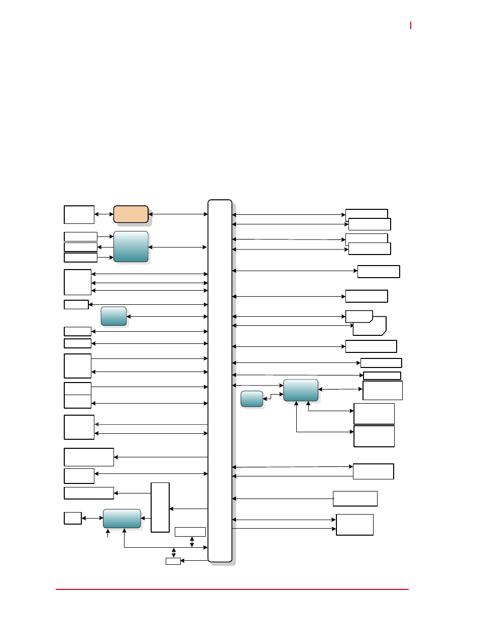
Block Diagram
Figure 1-1 presents a functional representation of the baseboard.
Figure 1-1: Functional Block Diagram
US B 1 _ B
US B 1 _ A
HDMI-J6
H D M I - R G B
S I L9 0 2 2
C o d e c
T LV 3 2 0 AI
C 2 3 B PW
L A N
T ra ns form er
314-
p
in
Co
n
n
e
ct
o
r
USB0
USB2
USB1
USB 2.0
SPI1
Level
Shift
buffers
HDMI
RGB 18/24-bit
Header
18/24-bit RGB TTL
GbE
RJ45
10/100/1000
SATA1
SATA Connector
eMMC/SD/SDIO 8-bit
Line OUT
Line IN
SPDIF
Header
SPI0
UART1 (4-pin)
UART3 (2-pin)
UART4 (2-pin)
DB9
Camera Input Control Signals
CAM3
I
2
C LCD
USB 2.0 OTG
PCIE_A (x1)
HDMI / (or DP)
Header
24-bit LVDS
SDMMC
SD/SDIO 4-bit
SDIO
CSI1 Camera Input
I
2
2
C CAM
I2S1
I2S1
I C GP
I2S2 / HDA
I2S3
SPDIF
Management Pins
MIC
DB9
UART2 (4-pin)
CAN1 (2-pin)
CSI0 Camera Input
LVDS 18/24-bit
Header
I
2
C HDMI_CTRL
USB 2.0
(4 ports)
PC1
Header
Vdd, BKL_EN, BKL_CTRL
Boot Select / Force Recovery
DIP switch (4)
Test point
Header
Watchdog Time Out
GPIO (12-pin)
miniPCIe x1
A Slot
PCIe x1 Slot
PCIE_WAKE#
Power ena ble /
dis a ble jum per
DB9
DB9
Header
Header
U S B H U B
S MS C
US B 2 5 1 4 i
USB1_C
miniPCIe x1
B Slot
DB9 (Dual)
G P S
Neo6
US B 1 _ D
G S e n s o r
MMA7660FCT
EEPROM 4K
RTC
VRTC
I2C_HDMI
LEC_BASE_blkDiag_b
CAM0
CAM1