17 power management (pw1), 18 spi0, 19 spi1 – ADLINK LEC-BASE R1 User Manual
Page 23
Interface Signals
17
LEC-BASE
2.1.17
Power Management (PW1)
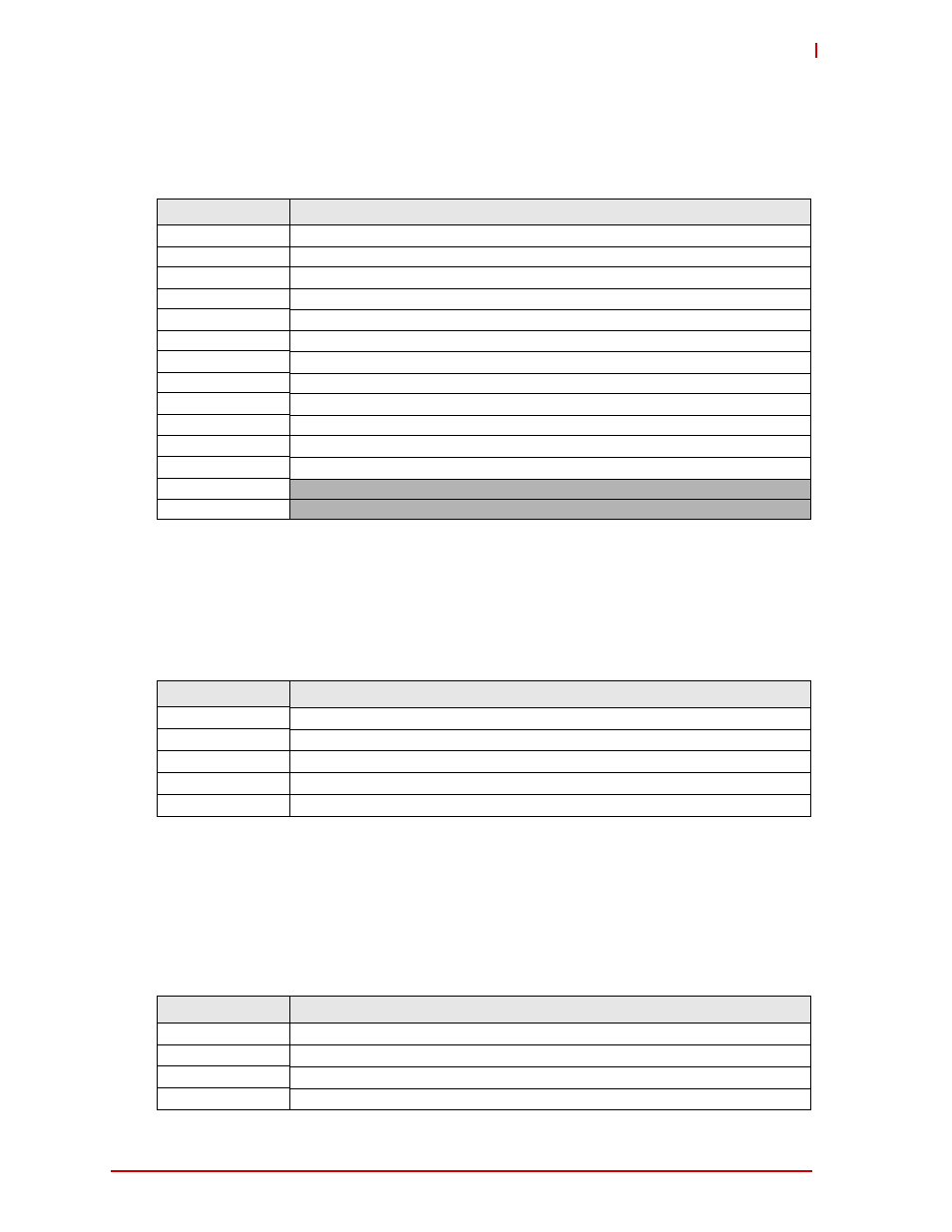
Table 2-21 lists the pin signals of the Power Management header, which provides 14 pins in 2
rows, odd/even pin sequence (1, 2), and 0.079" (2.00mm) pitch. These pins are connected
directly to the Power Management pins at the SMARC connector.
NOTE: Shaded table cells denote ground.
2.1.18
SPI0
Table 2-22 lists the pin signals of the System Packet Interface 0 header, which provides 5 pins in
a single row with 0.098" (2.50mm) pitch. These pins are connected to the SMARC connector
over the 3.3 volt level shifter.
NOTE: The signals for this header are defined by the module CPU as “SPI2”, but the header is
labelled “SPI0” on the board.
2.1.19
SPI1
Table 2-23 lists the pin signals of the System Packet Interface 1 header, which provides 4 pins in
a single row with 0.098" (2.50mm) pitch. These pins are connected to the SMARC connector
over the 3.3 volt level shifter.
Table 2-21: Power Management Signals (PWM1)
Pin #
Signal
1
WDT_TIME
2
VIN_PWR_nBAD
3
nLID
4
nCHARGING
5
nSLEEP
6
CHARGE_nPRSNT
7
nBATLOW
8
CHARGE_nSTBY
9
nTEST
10
CARRIED_PWR_ON
11
Not Connected
12
Not Connected
13
GND
14
GND
Table 2-22: System Packet Interface 0 Signals (SPI0)
Pin #
Signal
1
SPI2_CLK_3V (connected to SMARC pin P56)
2
SPI2_SOMI_3V (connected to SMARC pin P57)
3
SPI2_SIMO_3V (connected to SMARC pin P58)
4
SPI2_CS0_3V
(connected to SMARC pin P54)
5
SPI2_CS1_3V
(connected to SMARC pin P55)
Table 2-23: System Packet Interface 1 Signals (SPI1)
Pin #
Signal
1
SPI1_CS0_3V (connected to SMARC pin P43)
2
SPI1_CLK_3V (connected to SMARC pin P44)
3
SPI1_SOMI_3V (connected to SMARC pin P45)
4
SPI1_SIMO_3V
(connected to SMARC pin P46)