ADLINK LEC-BASE R1 User Manual
Page 13
Overview
7
LEC-BASE
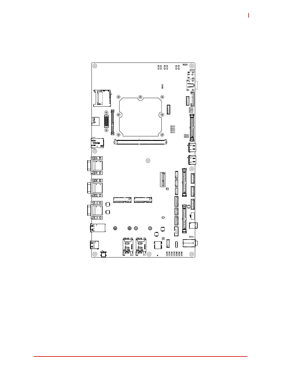
Figure 1-3: Connector Locations (Top Side)
JACK1
PWRON1
PWRON2
SD2
LED8
LED16
LED2
LED1
LED3
LED9
MINIPCIE1
MINIPCIE2
LED7
CN2
H25
CN4
LAN1
COM1
COM2
CAN1
USBC1
USB2
USB1
SIM1
SIM2
JP13
SPI0
SPI1
PC1
CAM3
CAM1
CAM0
PCIE1
J3
J10
J12
LED6
LED5
LED4
J8
J14
AJ1
SPDIF1
JP12
CN1
I2S3
I2S2
I2S1
J11
J1
S1
P1
J6
J9
(AFB1)
AFB2
SATA1
JP2
JP14
JP8
JP9
CN5
JP4
JP20
JP15
JP7
JP6
JP5
JP3
LED15
LED14
LED13
LED12
LED11
PWM1
JP21
JP10
JP1
1
ANT1
GPIO1
SW15
LEC-BASE_Baseboard_T
op_Conn_c
JP19
JP18
JP17
JP16
Key:
AFB2 - Alternate Function Block 2
AJ1 - Audio Jack
ANT1 - GPS Antenna
CAM0 - Camera 0
CAM1 - Camera 1
CAM3 - Camera 3
CAN1 - Controller Area Network (Dual Ports)
CN1 - 4-wire Resistive Touch Controller
CN2 - microSD (8 bits)
CN4 - Cell Charger/Battery Supply
CN5 - MiniDin DC Jack
COM1 - UART (Dual Ports)
COM2 - UART (Dual Ports)
PC1 - TTL Panel Control
PCIE1 - PCI Express
PWM1 - Power Management
PWRON1 - Power On
PWRON2 - Power On
SATA1 - SATA
SD2 - SD Card Slot
SIM1 - SIM Slot
SIM2 - SIM Slot
SPDIF1 - SPDIF OUT
SPI0 - System Packet Interface
SPI1 - System Packet Interface
SW15 - Reset Switch
USBC1 - USB
USB1 - Micro USB
USB2 - USB
NOTE: The larger black pins
each represent pin 1
LAN1 - Ehternet
LED1 - USB
LED2 - Mini PCIE1
LED3 - Mini PCIE2
LED4 - nLID
LED5 - nSLEEP
LED6 - nBATLOW
LED7 - SATA
LED8 - SD Card (4 bits)
LED9 - USB
LED11 - Cell Protection IC
LED12 - Cell Protection IC
LED13 - Cell Protection IC
LED14 - Cell Protection IC
LED15 - Cell Protection IC
LED16 - Power
MINIPCIE1 - PCIe Mini Card
MINIPCIE2 - PCIe Mini Card
JP4 - Battery Charger Enable
JP5 - Cell Charger Present
JP6 - Cell Charger Voltage
JP7 - Cell Protection IC
JP8 - LCD/LVDS Select
JP9 - LCD/LVDS Select
JP10 - LVDS Strobe
JP11 - LVDS Controller
JP12 - LVDS Backlight Control
JP13 - LVDS Panel Control
JP14 - LVDS Backlight Control
JP15 - Select I2C_HDMI for J11
JP16 - Boot Select
JP17 - Boot Select
JP18 - Boot Select
JP19 - Boot Select Recovery
JP20 - VIO Select
JP21 - DC-OUT
GPIO1 - General Purpose IO
H25 - Smart Battery
I2S1 - I2S 1
I2S2 - I2S 2
I2S3 - I2S 3
J1 - SMARC Interface
J3 - TTL LCD
J6 - HDMI1
J8 - LVDS LCD
J9 - Alternate Function Block 1
J10 - I2C
J11 - HDMI2
J12 - External Battery (RTC backup)
J14 - LVDS Control
JACK1 - DC Power In
JP2 - LCD Power Select
JP3 - Select I2C_LCD for J11