2 interface signals, 1 sd/emmc (afb2) interface, Sd/emmc (afb2) interface – ADLINK LEC-BASE R1 User Manual
Page 15: 2interface signals
Interface Signals
9
LEC-BASE
2
Interface Signals
This section provides the pin signals for all the non-standard user interfaces on the LEC-BASE.
Signal definitions for standard interfaces such as SATA, USB, PCIe, and DB9 serial connectors
can be found in their respective specification data sheets.
NOTE: The tables in this section define pin sequence using the method in the following exam-
ple: A 10-pin header with two rows of pins, using odd/even numbering, where pin 2 is directly
across from pin 1, is noted as 10 pins, 2 rows, odd/even pin sequence (1, 2).
2.1.1
SD/eMMC (AFB2) Interface
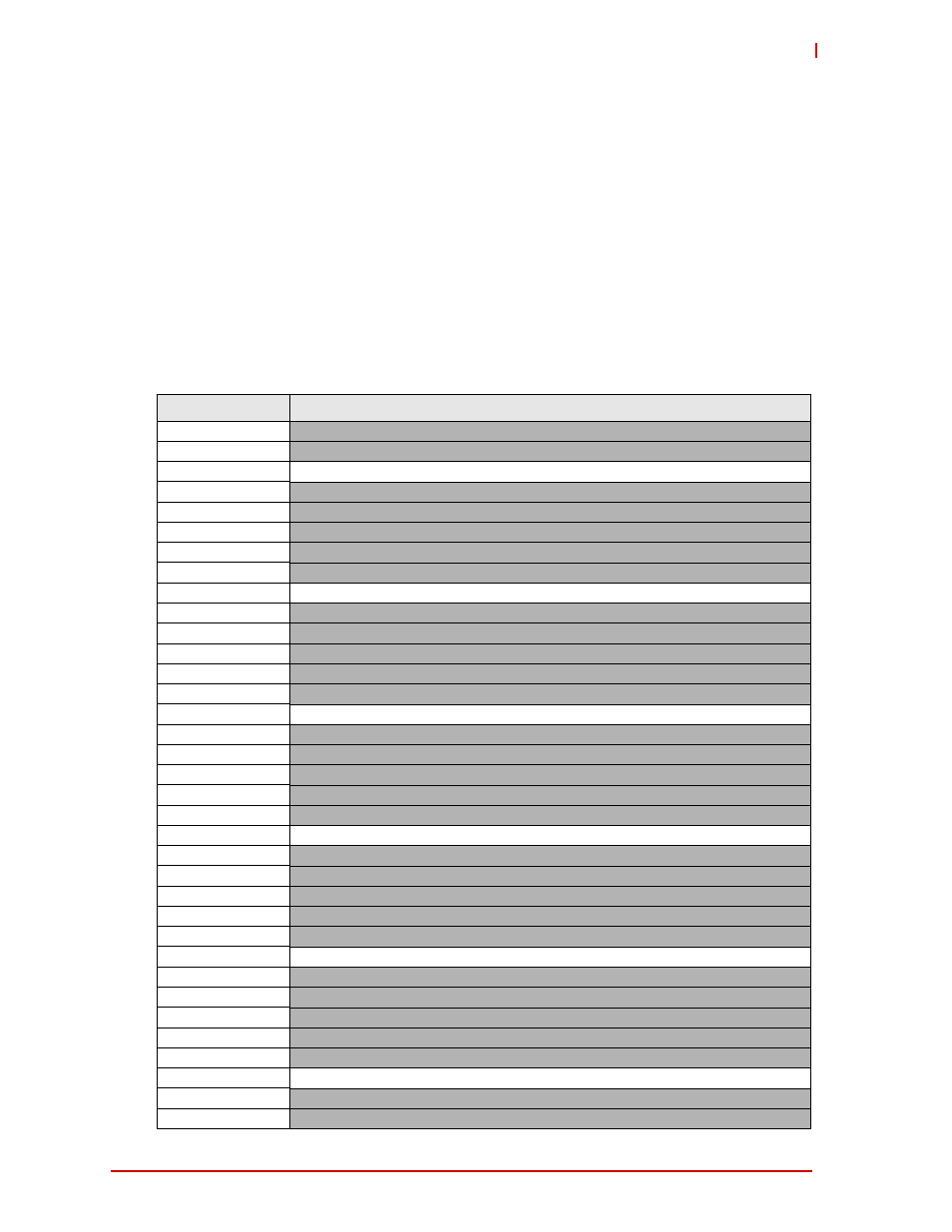
Table 2-4 lists the pin signals of the SD Card ground plane socket, which provides 60-pins, 2
rows, odd/even pin sequence (1, 2) with 0.02" (0.50mm) pitch. These signals are connected to
the SD/eMMC interface at pins S26 through S36 of the SMARC connector over a 3.3 volt level
shifter.
Table 2-4: SD/eMMC (AFB2) Interface Pin Signals
Pin #
Signal
1
GND
2
GND
3
MMC2_D0_3V
4
GND
5
GND
6
GND
7
GND
8
GND
9
MMC2_D1_3V
10
GND
11
GND
12
GND
13
GND
14
GND
15
MMC2_D2_3V
16
GND
17
GND
18
GND
19
GND
20
GND
21
MMC2_D3_3V
22
VDD_3V3
23
GND
24
GND
25
GND
26
GND
27
MMC2_D4_3V
28
VDD_3V3
29
GND
30
GND
31
GND
32
GND
33
MMC2_D5_3V
34
GND
35
GND