20 lvds – ADLINK LEC-BASE R1 User Manual
Page 24
18
Interface Signals
2.1.20
LVDS
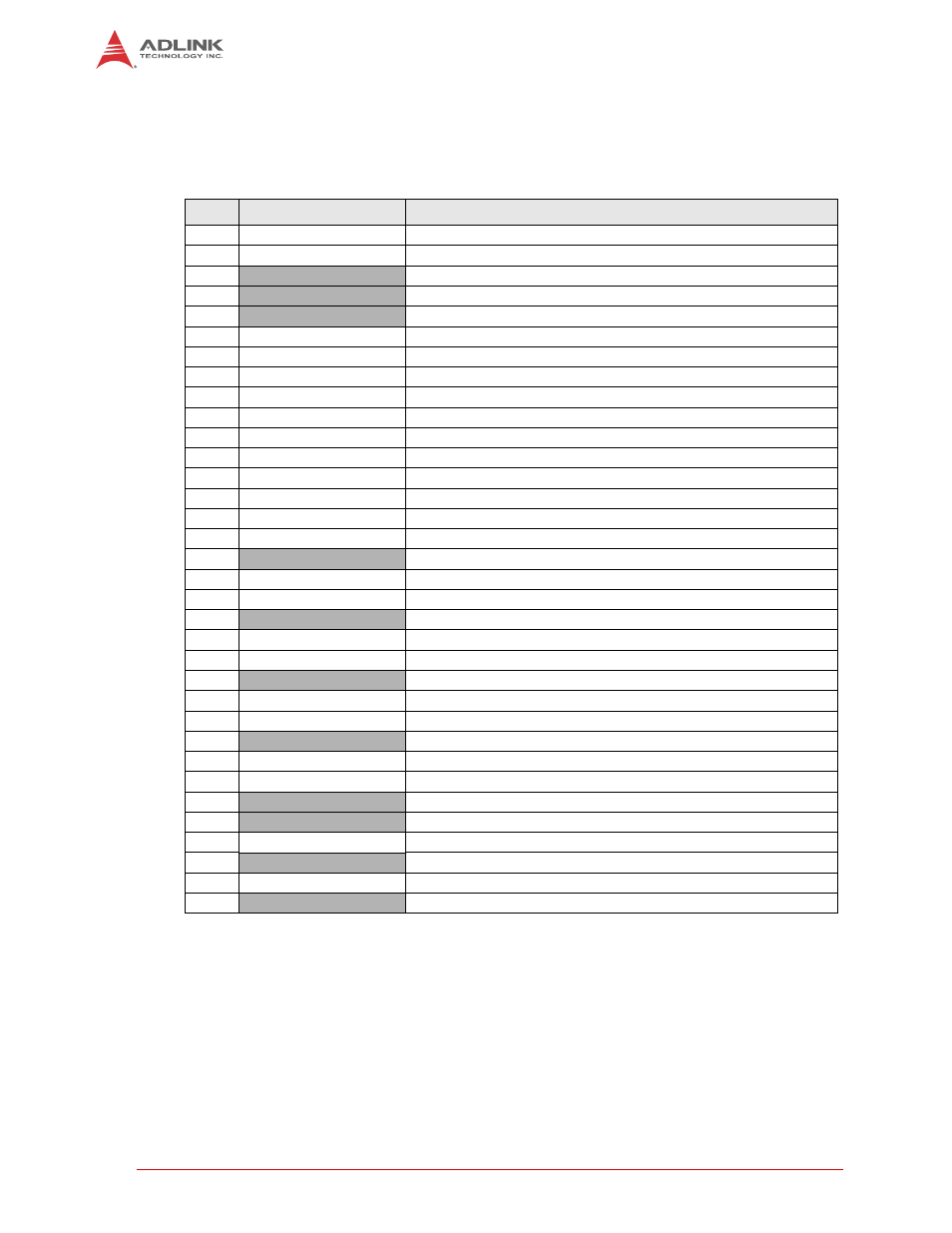
Table 2-24 lists the pin signals of the LVDS header which provides 34-pins, 2 rows, odd/even pin
sequence (1, 2) with 0.079" (2.0mm) pitch. These pins are connected directly to the LVDS inter-
face at the SMARC connector.
NOTE: The shaded table cells denote power or ground.
Table 2-24: LVDS Interface Pin Signals (J8)
Pin #
Signal
Description
1
I2C_LCD_DAT
System Management Data
2
I2C_LCD_CK
System Management Clock
3
PNL_PWR
Panel Power [JP2 (1-2) for 5V, (2-3) for 3.3V]
4
PNL_PWR
Panel Power [JP2 (1-2) for 5V, (2-3) for 3.3V]
5
GND
Ground
6
LVDS_A0N
Data Negative Output
7
LVDS_A0P
Data Positive Output
8
LCD_BLPWM_3V
Backlight PWM(3.3V)
9
LVDS_A1N
Data Negative Output
10
LVDS_A1P
Data Positive Output
11
LVDS_BL_EN
Backlight Enable, if supported
12
LVDS_A2P
Data Positive Output
13
LVDS_A2N
Data Negative Output
14
eDP_HPD
Display Port Control
15
LVDS_CKN
Clock Negative
16
LVDS_CKP
Clock Positive
17
PNL_PWR
Panel Power [JP2 (1-2) for 5V, (2-3) for 3.3V]
18
LVDS_A3P
Data Positive Output
19
LVDS_A3N
Data Negative Output
20
GND
Ground
21
LCD_DUAL_PCK
LCD Dual Display Pixel Clock
22
LCD_BKLTPWM_5V
LCD Backlight Power Management (5V)
23
GND
Ground
24
LCD_BKEN_5V
LCD Backlight Enable (5V)
25
SEL68
Connected over 4.7 KOhm to GND
26
GND
Ground
27
R/L
Connected over 4.7 KOhm to 3.3V
28
NC
Not Connected
29
GND
Ground
30
VDD_3V3
3.3V Supply
31
U/D
Connected over 4.7 KOhm to 3.3V
32
VDD_5V
5V Supply
33
REV
Connected over 4.7 KOhm to 3.3V
34
GND
Ground