13 i2c (j10), 14 battery (j12), 15 lvds control (j14) – ADLINK LEC-BASE R1 User Manual
Page 22: 16 ttl panel control (pc1)
16
Interface Signals
2.1.13
I2C (J10)
Table 2-17 lists the pin signals of the I2C header, which provides 2 pins with 0.049" (1.25mm)
pitch. These pins are connected to the SMARC connector over the 3.3 volt level shifter.
2.1.14
Battery (J12)
Table 2-18 lists the pin signals of the battery header, which provides 2 pins with 0.049"
(1.25mm) pitch.
NOTE: Shaded table cells denote power or ground.
2.1.15
LVDS Control (J14)
Table 2-19 lists the pin signals of the Smart Battery header, which provides 8 pins in two rows
with odd/even pin sequence (1,2) and 0.01" (2.54mm) pitch.
NOTE: Shaded table cells denote ground.
2.1.16
TTL Panel Control (PC1)
Table 2-20 lists the pin signals of the TTL Panel Control header, which provides 6 pins in a sin-
gle row with 0.098" (2.50mm) pitch. These pins are connected directly to the display control pins
at the SMARC connector.
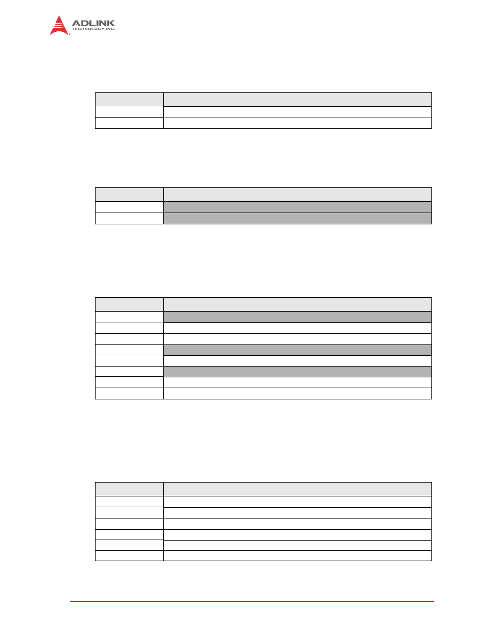
Table 2-17: I2C Signals (J10)
Pin #
Signal
1
I2C_GP_DAT_3V (connected to SMARC pin S48)
2
I2C_GP_CK_3V (connected to SMARC pin S49)
Table 2-18: Battery Signals (J12)
Pin #
Signal
1
V_RTC
2
GND
Table 2-19: LVDS Control Signals (J14)
Pin #
Signal
1
GND
2
PNLPWR (display supply voltage, selectable with JP13)
3
LVDS_BKL_CTRL (backlight control, selectable with JP12)
4
GND
5
LCD_nEN (backlight enable)
6
GND
7
Not Connected
8
BLPWR
(backlight supply voltage, selectable with JP14)
Table 2-20: LVDS Control Signals (PC1)
Pin #
Signal
1
LCD_DE (connected over the 3.3 volt level shifter)
2
LCD_BKLT_PWM
3
LCD_VDD_EN
4
Not Connected
5
Not Connected
6
LCD_RESET (Active Low)