7 gpio1, 8 smart battery (h25), Gpio1 – ADLINK LEC-BASE R1 User Manual
Page 19: Smart battery (h25)
Interface Signals
13
LEC-BASE
2.1.7
GPIO1
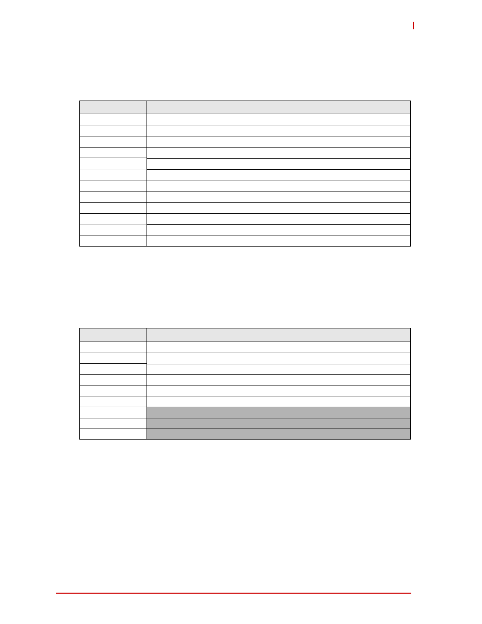
Table 2-11 lists the pin signals of the General Purpose IO header, which provides 12 pins in 2
rows, odd/even pin sequence (1, 2), and 0.079" (2.00mm) pitch. These pins are connected to
the SMARC connector over the 3.3 volt level shifter.
NOTE: Signal names relative only to the LEC-3517 module.
2.1.8
Smart Battery (H25)
Table 2-12 lists the pin signals of the Smart Battery header, which provides 9 pins in a single row
with 0.079" (2.00mm) pitch. These signals are connected to and controlled by the onboard
LTC1760 smart battery charger controller.
NOTE: Shaded table cells denote ground.
Table 2-11: General Purpose IO (GPIO1)
Pin #
Signal
1
GPIO_28_3V (connected to SMARC pin P119)
2
CAM0_nPWREN_3V
(connected to SMARC pin P108)
3
GPIO_29_3V (connected to SMARC pin P112)
4
CAM1_nPWREN_3V
(connected to SMARC pin P109)
5
GPIO_177_3V (connected to SMARC pin P116)
6
CAM0_nRST_3V
(connected to SMARC pin P110)
7
GPIO_54_3V (connected to SMARC pin P117)
8
CAM1_nRST_3V
(connected to SMARC pin P111)
9
GPIO_55_3V (connected to SMARC pin P113)
10
CAM_FLD_3V
(connected to SMARC pin P115)
11
GPIO_56_3V (connected to SMARC pin P114)
12
GPIO_27_3V (connected to SMARC pin P118)
Table 2-12: Smart Battery (H25)
Pin #
Signal
1
+VE (battery and charging voltage)
2
+VE (battery and charging voltage)
3
+VE (battery and charging voltage)
4
1760_SCL1
(I2C bus from LTC1760 charger controller)
5
1760_SDA1 (I2C bus from LTC1760 charger controller)
6
TH1 (Thermistor Force/Sense connection to LTC1760 charger controller)
7
GND
8
GND
9
GND