Power and ground – ADLINK Express-CVC User Manual
Page 25
Express-CVC
Page 25
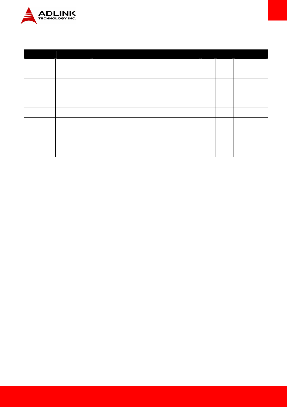
3.3.16. Power and Ground
Signal
Pin
Description
I/O
PU/PD
Comment
VCC_12V A104-A109
B104-B109
Primary power input: +12V nominal (5 ~ 19V). See section 7
“Electrical Specifications“ for allowable input range. All available
VCC_12V pins on the connector(s) shall be used.
P
5~20
V
VCC_5V_SBY
B84-B87
Standby power input: +5.0V nominal. See section 7 “Electrical
Specifications“ for allowable input range. If VCC5_SBY is used,
all available VCC_5V_SBY pins on the connector(s) shall be used.
Only used for standby and suspend functions. May be left
unconnected if these functions are not used in the system design.
P
5Vsb
±5%
VCC_RTC
A47
Real-time clock circuit-power input. Nominally +3.0V.
P
GND
A1, A11, A21, A31,
A41, A51, A57, A66,
A80, A90, A96,
A100, A110, B1,
B11, B21 ,B31, B41,
B51, B60, B70, B80,
B90, B100, B110
Ground - DC power and signal and AC signal return path.
P
- USB-1901 (84 pages)
- USB-1210 (54 pages)
- USB-2401 (60 pages)
- USB-7230 (50 pages)
- USB-2405 (56 pages)
- DAQe-2010 (92 pages)
- DAQe-2204 (100 pages)
- DAQe-2213 (94 pages)
- DAQe-2501 (74 pages)
- PXI-2010 (84 pages)
- PXI-2020 (60 pages)
- PXI-2501 (62 pages)
- cPCI-9116 (98 pages)
- ACL-8112 Series (93 pages)
- ACL-8112 Series (94 pages)
- ACL-8112 Series (92 pages)
- ACL-8216 (75 pages)
- ACL-8111 (61 pages)
- PCM-9112+ (10 pages)
- PCM-9112+ (94 pages)
- cPCI-6216V (47 pages)
- ACL-6126 (28 pages)
- ACL-6128A (40 pages)
- PCM-6308V+ (52 pages)
- PCM-6308V+ (4 pages)
- PCI-7444 (82 pages)
- PCI-7434 (48 pages)
- PCI-7234 (56 pages)
- PCI-7260 (66 pages)
- PCI-7258 (38 pages)
- PCI-7256 (48 pages)
- PCI-7250 (48 pages)
- LPCI-7250 (48 pages)
- PCI-7396 (65 pages)
- PCI-7296 (59 pages)
- PCI-8554 (67 pages)
- PCIe-7360 (94 pages)
- PCIe-7350 (86 pages)
- PCIe-7300A (114 pages)
- PCIe-7200 (51 pages)
- PCI-7300A (112 pages)
- PCI-7300A (83 pages)
- PCI-7200 (96 pages)
- cPCI-7300 (82 pages)
- cPCI-7300 (83 pages)