4 cd signal descriptions, 1 pata ide, 2 pci – ADLINK Express-HL2 User Manual
Page 25: Cd signal descriptions
Express-HL2
Page 25
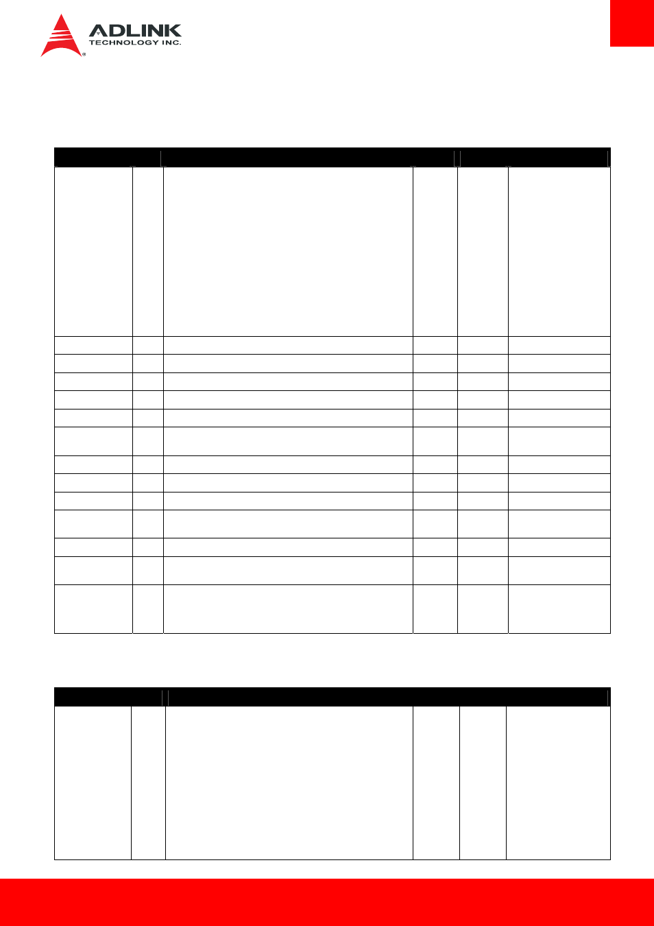
3.4 CD Signal Descriptions
3.4.1
PATA IDE
Signal
Pin # Description
I/O
PU/PD
Comment
IDE_D0
IDE_D1
IDE_D2
IDE_D3
IDE_D4
IDE_D5
IDE_D6
IDE_D7
IDE_D8
IDE_D9
IDE_D10
IDE_D11
IDE_D12
IDE_D13
IDE_D14
IDE_D15
D7
C10
C8
C4
D6
D2
C3
C2
C6
C7
D3
D4
D5
C9
C12
C5
Bidirectional data to / from IDE device.
I/O 3.3V
IDE_A0
D13
Address lines to IDE device.
O 3.3V
IDE_A1
D14
Address lines to IDE device.
O 3.3V
IDE_A2
D15
Address lines to IDE device.
O 3.3V
IDE_IOW#
D9
I/O write line to IDE device. Data latched on trailing (rising) edge.
O 3.3V
IDE_IOR#
C14
I/O read line to IDE device.
O 3.3V
IDE_REQ
D8
IDE Device DMA Request. It is asserted by the IDE device to request a
data transfer.
I 3.3V
IDE_ACK#
D10
IDE Device DMA Acknowledge.
O 3.3V
IDE_CS1#
D16
IDE Device Chip Select for 1F0h to 1FFh range.
O 3.3V
IDE_CS3#
D17
IDE Device Chip Select for 3F0h to 3FFh range.
O 3.3V
IDE_IORDY
C13
IDE device I/O ready input. Pulled low by the IDE device to extend the
cycle.
I 3.3V
PU 4k7 3.3V
IDE_RESET#
D18
Reset output to IDE device, active low.
O 3.3V
IDE_IRQ
D12
Interrupt request from IDE device.
I 3.3V
PD 10k
shall
IDE_CBLID#
D77
Input from off-module hardware indicating the type of IDE cable being
used. High indicates a 40-pin cable used for legacy IDE modes. Low
indicates that an 80-pin cable with interleaved grounds is used. Such a
cable is required for Ultra-DMA 66, 100 and 133 modes.
I 3.3V
3.4.2
PCI
Signal
Pin #
Description
I/O
PU/PD
Comment
PCI_AD0
PCI_AD1
PCI_AD2
PCI_AD3
PCI_AD4
PCI_AD5
PCI_AD6
PCI_AD7
PCI_AD8
PCI_AD9
PCI_AD10
PCI_AD11
PCI_AD12
C24
D22
C25
D23
C26
D24
C27
D25
C28
D27
C29
D28
C30
PCI bus multiplexed address and data lines
I/O 3.3V