6 pci express, 7 express card, 8 lpc bus – ADLINK Express-HL2 User Manual
Page 19
Express-HL2
Page 19
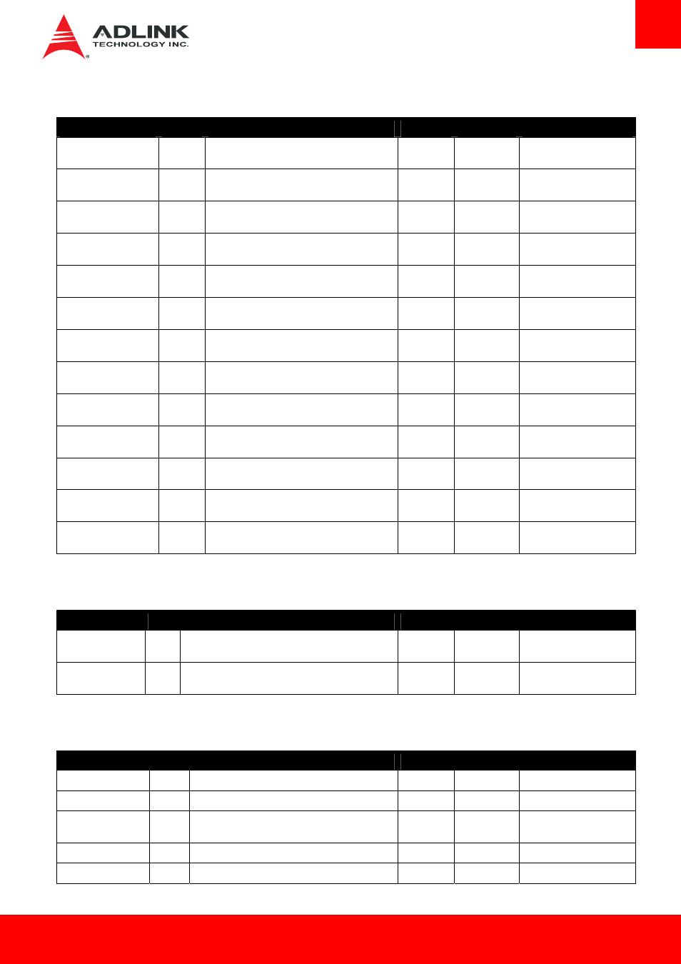
3.3.6
PCI Express
Signal
Pin #
Description
I/O
PU/PD
Comment
PCIE_TX0+
PCIE_TX0-
A68
A69
PCI Express channel 0, Transmit Output
differential pair.
O PCIE
AC coupled on Module
PCIE_RX0+
PCIE_RX0-
B68
B69
PCI Express channel 0, Receive Input
differential pair.
I PCIE
AC coupled off Module
PCIE_TX1+
PCIE_TX1-
A64
A65
PCI Express channel 1, Transmit Output
differential pair.
O PCIE
AC coupled on Module
PCIE_RX1+
PCIE_RX1-
B64
B65
PCI Express channel 1, Receive Input
differential pair.
I PCIE
AC coupled off Module
PCIE_TX2+
PCIE_TX2-
A61
A62
PCI Express channel 2, Transmit Output
differential pair.
O PCIE
AC coupled on Module
PCIE_RX2+
PCIE_RX2-
B61
B62
PCI Express channel 2, Receive Input
differential pair.
I PCIE
AC coupled off Module
PCIE_TX3+
PCIE_TX3-
A58
A59
PCI Express channel 3, Transmit Output
differential pair.
O PCIE
AC coupled on Module
PCIE_RX3+
PCIE_RX3-
B58
B59
PCI Express channel 3, Receive Input
differential pair.
I PCIE
AC coupled off Module
PCIE_TX4+
PCIE_TX4-
A55
A56
PCI Express channel 4, Transmit Output
differential pair.
O PCIE
AC coupled on Module
PCIE_RX4+
PCIE_RX4-
B55
B56
PCI Express channel 4, Receive Input
differential pair.
I PCIE
AC coupled off Module
PCIE_TX5+
PCIE_TX5-
A52
A53
PCI Express channel 5, Transmit Output
differential pair.
O PCIE
AC coupled on Module
PCIE_RX5+
PCIE_RX5-
B52
B53
PCI Express channel 5, Receive Input
differential pair.
I PCIE
AC coupled off Module
PCIE_CLK_REF+
PCIE_CLK_REF-
A88
A89
PCI Express Reference Clock output for all PCI
Express and PCI Express Graphics Lanes.
O PCIE
3.3.7
Express Card
Signal
Pin #
Description
I/O
PU/PD
Comment
EXCD0_CPPE#
EXCD1_CPPE#
A49
B48
PCI ExpressCard: PCI Express capable card request
I 3.3V
PU 10k 3.3V
EXCD0_PERST#
EXCD1_PERST#
A48
B47
PCI ExpressCard: reset
O 3.3V
3.3.8
LPC Bus
Signal
Pin #
Description
I/O
PU/PD
Comment
LPC_AD[0:3]
B4-B7
LPC multiplexed address, command and data bus
I/O 3.3V
LPC_FRAME#
B3
LPC frame indicates the start of an LPC cycle
O 3.3V
LPC_DRQ0#
LPC_DRQ1#
B8
B9
LPC serial DMA request
I 3.3V
LPC_SERIRQ
A50
LPC serial interrupt
I/O OD 3.3V PU 8k2 3.3V
LPC_CLK
B10
LPC clock output - 33MHz nominal
O 3.3V