2 vr assignment, 3 internal reference source adjustment – ADLINK ACL-6128A User Manual
Page 36
28
• Calibration
5.2 VR
Assignment
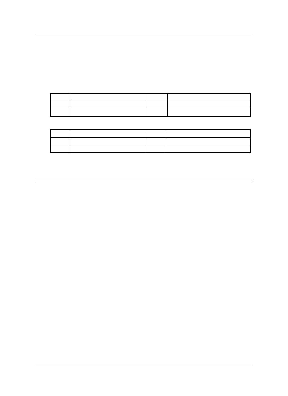
There are twelve variable resistors (VR) on the ACL-6128A board to allow
users to make accurate adjustment on two D/A channels. VR1 to VR6 belong
to CH1, and VR7 to VR12 belongs to CH2. The detailed functionality of each
VR is listed below:
CH1‘s VR
VR1 (-10V) Internal reference
VR2 (-5V) Internal reference
VR3 Gain Adjustment
VR4 Unipolar Offset
VR5 Current Sink Offset (4mA)
VR6 Bipolar Offset
CH2‘s VR
VR7 (-10V) Internal reference
VR8 (-5V) Internal reference
VR9 Gain Adjustment
VR10 Unipolar Offset
VR11 Current Sink Offset (4mA) VR12 Bipolar Offset
There are two testing points (TP1 and TP2) on the board, which are used for
calibration the ACL-6128A. TP1 is for CH1, and TP2 is for CH2.
5.3 Internal Reference Source Adjustment
The Internal Reference Source adjustment can ensure that the internal
reference voltages of the ACL-6128A can offer very accurate voltage source—-
5V and -10V.
1.
Ground the black probe of the voltmeter.
2.
Connect the other probe to TP1 (for testing CH1), or TP2 (for testing
CH2).
Change the jumper to JP3 (for CH1) or JP7 (for CH2), trim VR1 (for
CH1) until the voltmeter reads -10V, trim VR7 (for CH2) until the
voltmeter also reads -10V.
3.
Change the jumper to JP3 (for CH1) or JP7 (for CH2), trim VR2 (for
CH1) until the voltmeter reads -5V, trim VR8 (for CH2) until the
voltmeter also reads -5V.