Figure 4-11, Waveform generation for two channel update, Figure 4-12 – ADLINK USB-1903 User Manual
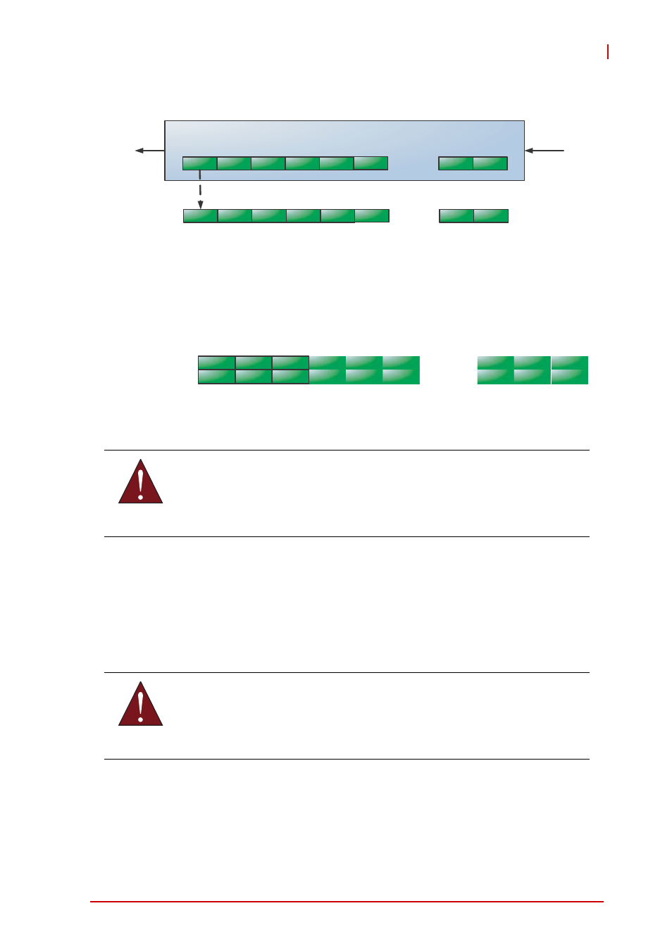
Page 63: Fifo data in/out structure, Data format in fifo is shown, Figure 4-12: fifo data in/out structure
Operation
49
USB-1900 Series
Figure 4-11: Waveform Generation for Two Channel Update
Data format in FIFO is shown.
Figure 4-12: FIFO Data In/Out Structure
With hardware-based waveform generation, D/A conversions
are updated automatically by the FPGA rather than by the
application software. Compared with conventional soft-
ware-based waveform generation, the precise hardware timing
control guarantees non-distorted waveform generation based
on a given and fixed time interval.
Waveform Generation Clock Source
When the onboard DAC receives a conversion clock signal, a
D/A update is triggered. The USB-1902/1903 update clock
originates with the 80 MHz internal hardware timer.
WARNING:
While waveform patterns exceeding the 10k samples are also
supported in continuous mode, the output data may not be
updated in the fixed time interval if the USB bus is busy.
WARNING:
In waveform generation mode, both DACs must be configured
in the same mode. However, individual DACs can be disabled.
FFFF
0000
FFFE
0001
FFFD
FF00
00FF
CH0
CH1
CH0
CH1
CH0
CH0
CH1
0002
CH1
512 Samples Data FIFO
Da
ta
I
n
Dat
a
O
u
t
16 Bit Hex Data Format
……
……
Destination
Channel
FFFF
0000
FFFE
0001
FFFD
0002
FF00
00FF
DA Channel 0
DA Channel 1
…………
…………