2 a/d conversion, A/d conversion, Figure 4-1 – ADLINK USB-1903 User Manual
Page 50: Functional block diagram (usb-1902), Fpga
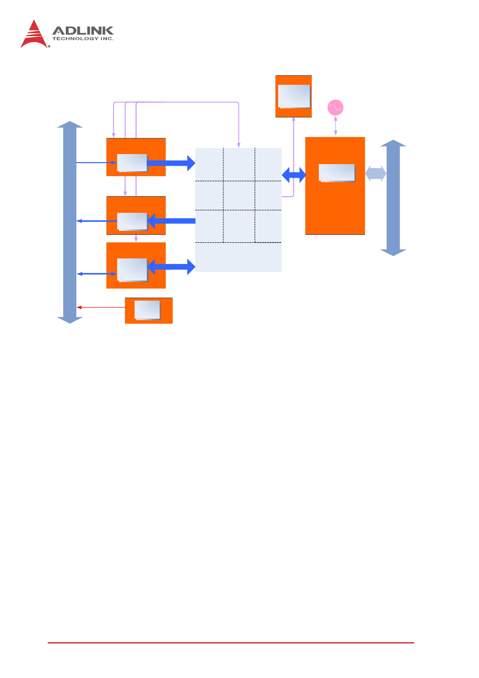
36
Operation
Figure 4-1: Functional Block Diagram (USB-1902)
4.2
A/D Conversion
When using an A/D converter, the properties of the signal to be
measured must be considered and a channel and connection of
signals to the module selected. Please see Section 2.3: Analog
Input Signal Connection. As well, A/D signal configuration,
including channel, gain, and signal type must be defined and set.
A/D acquisition is initiated by a predefined trigger source. Data
acquisition will commence once a trigger condition is matched.
After A/D conversion, A/D data is buffered in a data FIFO for
transfer into system memory for further processing.
40
P
CO
N
N
E
C
T
O
R
IN
TER
F
A
C
E
FPGA
C
a
libr
a
ti
on
dat
a
80
51
Co
re
fu
n
cti
o
n
AFI
General Timer/
Counter
Control signal
DI DO Circuit
General
Timer/
Counter
PWM
DIO circuit
16 Bit DAC
DAC Circuit
16 Bit ADC
AD7610
ADC Front end
2AO
8DI 4DO
16AI
US
B
IN
T
E
R
F
A
C
E
Cypress
CY7C68013A
24MHz XTAL
8051 Core
12/24/48MHz
PWM
Digital I/O,
General Timer/Counter,
Pulse Generation
AO da
ta
co
nt
ro
l
AI
D
a
ta
an
d
Co
nt
ro
l
DATA
EEPROM
EEPROM
AI
C
a
libr
a
ti
on
Co
n
tr
o
l
AO
C
a
lib
ra
ti
o
n
Co
n
tro
l
Ot
h
e
rs
Power
Power
circuit
+-13V
+5V Supply