5 generating a summary page and bom (system power), 1 exploring the system power tool summary page – Maxim Integrated EE-Sim User Manual
Page 31
page
31
EE-Sim User Guide
4.4.2 Editing the Group/Rail Assignments and Viewing the Timing
Diagrams
Perform these steps to edit the group/rail assignments and generate timing
diagrams.
1. Open a system power design and click the
Sequencing tab.
2. Verify that you have added at least one sequencer.
3. Expand the
Group/Rail Assignment section. The color-coded FPGA
Groups and Rail(s) data appear only when you have added at least one
sequencer.
4. For each FPGA Group and rail or pin:
a. Choose a sequencer reference designation from the
Sequencer
field.
b. Enter a
Delay On value in milliseconds. This is the delay from t = 0
seconds before power is applied to the rail.
c. Enter a
Delay Off value in milliseconds. This is the delay from t = 0
seconds before power is terminated to the rail.
5. Click
Apply Changes.
6. Expand the
Timing Diagram section and examine the Delay On and
Delay Off graphs.
7. (Optional) Position your mouse over a data point in the graph to view its
FPGA group, voltage out, and delay in milliseconds.
8. Click
Save.
4.5 Generating a Summary Page and BOM (System Power)
4.5.1 Exploring the System Power Tool Summary Page
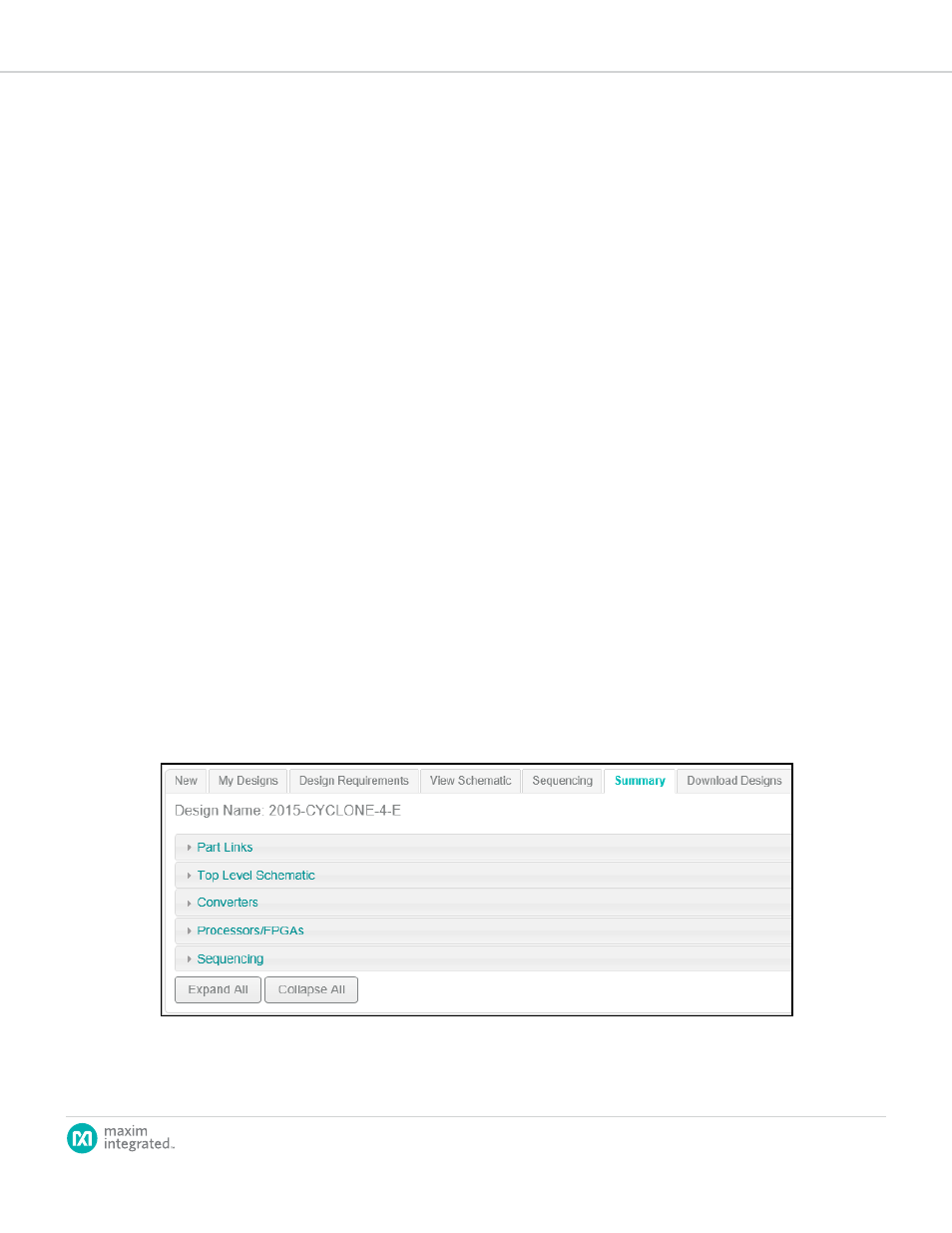
1. Open a system power design and click the Summary tab.
2. Scroll down to the bottom of the Summary page and click Collapse All.
The page shows the five sections of the Summary page: