Maxim Integrated DS80C390 User Manual
Page 6
DS80C390
6 of 58
110199
13
22
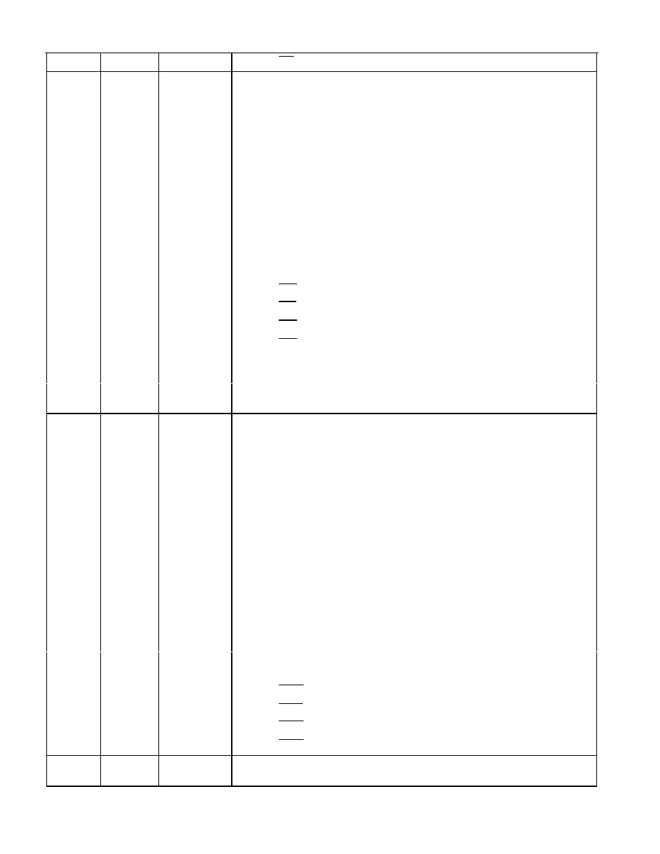
P3.7
RD
External Data Memory Read Strobe
34-27
45, 44,
42-37
P4.0-P4.7
Port 4 - I/O. Port 4 can function as an 8-bit bi-directional I/O port,
and as the source for external address and chip enable signals for
program and data memory. Port pins are configured as I/O or
memory signals via the P4CNT register. The reset condition of
Port 1 is all bits at logic 1 via a weak pullup. The logic 1 state also
serves as an input mode, since external circuits writing to the port
can overdrive the weak pullup. When software clears any port pin
to 0, the device activates a strong pulldown that remains on until
either a 1 is written to the port pin or a reset occurs. Writing a 1
after the port has been at 0 will activate a strong transition driver,
followed by a weaker sustaining pullup. Once the momentary
strong driver turns off, the port once again becomes the output (and
input) high state.
Port
Alternate Function
34
45
P4.0
CE0
Program Memory Chip Enable 0
33
44
P4.1
CE1
Program Memory Chip Enable 1
32
42
P4.2
CE2
Program Memory Chip Enable 2
31
41
P4.3
CE3
Program Memory Chip Enable 3
30
40
P4.4
A16 Program/Data Memory Address 16
29
39
P4.5
A17 Program/Data Memory Address 17
28
38
P4.6
A18 Program/Data Memory Address 18
27
37
P4.7
A19 Program/Data Memory Address 19
21-14
31-27,
25-23
P5.0-P5.7
Port 5 - I/O. Port 5 can function as an 8-bit bi-directional I/O port,
the CAN interface, or as peripheral enable signals. Setting the
SP1EC bit will relocate the RXD1 and TXD1 functions to P5.3-
P5.2 as described in the User’s Guide.
The reset condition of Port 1 is all bits at logic 1 via a weak pullup.
The logic 1 state also serves as an input mode, since external
circuits writing to the port can overdrive the weak pullup. When
software clears any port pin to 0, the device activates a strong
pulldown that remains on until either a 1 is written to the port pin or
a reset occurs. Writing a 1 after the port has been at 0 will activate
a strong transition driver, followed by a weaker sustaining pullup.
Once the momentary strong driver turns off, the port once again
becomes the output (and input) high state.
Port
Alternate Function
21
31
P5.0
C0TX CAN0 Transmit Output
20
30
P5.1
C0RX CAN0 Receive Input
19
29
P5.2
C1RX CAN1 Receive Input (optional RXD1)
18
28
P5.3
C1TX CAN1 Transmit Output (optional TXD1)
17
27
P5.4
PCE0
Peripheral Chip Enable 0
16
25
P5.5
PCE1
Peripheral Chip Enable 1
15
24
P5.6
PCE2
Peripheral Chip Enable 2
14
23
P5.7
PCE3
Peripheral Chip Enable 3
9, 26,
43, 60
NC - Reserved. These pins are reserved for use with future
devices in this family and should not be connected.