Internal movx sram, Internal movx sram configuration table 4 – Maxim Integrated DS80C390 User Manual
Page 13
DS80C390
13 of 58
110199
INTERNAL MOVX SRAM
The DS80C390 contains 4kB of SRAM that can be configured as user accessible MOVX memory,
program memory, or optional stack memory. The specific configuration and locations are governed by the
Internal Data Memory Configuration bits (IDM1, IDM0) in the Memory Control Register (MCON;C6h).
Note that when the SA bit (ACON.2) is set, the first 1kB of the MOVX data memory is reserved for use
by the 10-bit expanded stack. Internal memory accesses will not generate
WR
,
RD
, or
PSEN
strobes.
The DS80C390 can configure its 4kB of internal SRAM as combined program and data memory. This
allows the application software to execute self-modifiable code. The technique loads the 4kB SRAM
with bootstrap loader software, and then modifies the IDM1 and IDM0 bits to map the 4kB starting at
memory location 40000h. This allows the system to run the bootstrap loader without disturbing the 4 MB
external memory bus, making the device in-system reprogrammable for Flash or NV RAM.
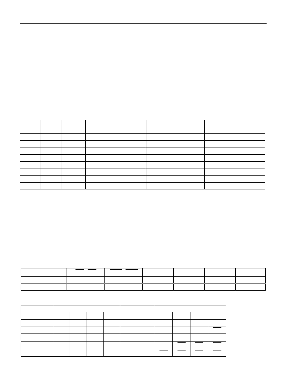
INTERNAL MOVX SRAM CONFIGURATION Table 4
IDM1
IDM0
CMA
MOVX Data Memory
CAN Message
Memory
Shared Program /Data
Memory
0
0
0
00F000h-00FFFFh
00EE00h-00EFFFh
- -
0
0
1
00F000h-00FFFFh
401000h-4011FFh
- -
0
1
0
000000h-000FFFh
00EE00h-00EFFFh
- -
0
1
1
000000h-000FFFh
401000h-4011FFh
- -
1
0
0
400000h-400FFFh
00EE00h-00EFFFh
- -
1
0
1
400000h-400FFFh
401000h-4011FFh
- -
1
1
0
- -
00EE00h-00EFFFh
400000h-400FFFh*
1
1
1
- -
401000h-4011FFh
400000h-400FFFh*
*10-bit expanded stack not available in Shared Program /Data Memory mode.
EXTERNAL MEMORY ADDRESSING
The enabling and mapping of the chip enable signals is done via the Port 4 Control Register (P4CNT;92h)
and Memory Control Register (MCON; 96h); The Extended Address and Chip Enable Generation Table
shows which chip enable and address line signals are active on Port 4. Following reset, the device will be
configured with P4.7-P4.4 as address lines and P4.3-P4.0 configured as
0
-
CE3
, with the first program
fetch being performed from 00000h with
CE0
active. The following tables illustrate which memory
ranges are controlled by each chip enable as a function of which address lines are enabled.
EXTERNAL MEMORY ADDRESSING PIN ASSIGNMENTS Table 5
Address/Data Bus
CE3
-
CE0
PCE3
-
PCE0
Addr 19-16 Addr 15-8
Addr 7-0
Data Bus
Multiplexed
P4.3-P4.0
P5.7-P5.4
P4.7-P4.4
P2
P0
P0
Demultiplexed
P4.3-P4.0
P5.7-P5.4
P4.7-P4.4
P2
P1
P0
EXTENDED ADDRESS AND CHIP ENABLE GENERATION Table 6
Port 4 Pin Function
Port 4 Pin Function
P4CNT.5-3
P4.7
P4.6
P4.5
P4.4
P4CNT.2-0
P4.3
P4.2
P4.1
P4.0
000
I/O
I/O
I/O
I/O
000
I/O
I/O
I/O
I/O
100
I/O
I/O
I/O
A16
100
I/O
I/O
I/O
CE0
101
I/O
I/O
A17
A16
101
I/O
I/O
CE1
CE0
110
I/O
A18
A17
A16
110
I/O
CE2
CE1
CE0
111(default)
A19
A18
A17
A16
111(default)
CE3
CE2
CE1
CE0