Typical i, Versus frequency – Maxim Integrated DS80C390 User Manual
Page 33
DS80C390
33 of 58
110199
NOTES FOR DC ELECTRICAL CHARACTERISTICS:
1. Active current measured with 40 MHz clock source on XTAL1, V
CC
=RST= 5.5 V, all other pins
disconnected.
2. Idle mode current measured with 40 MHz clock source on XTAL1, V
CC
= 5.5 V, RST=
EA
=V
SS
, all
other pins disconnected.
3. Stop mode current measured with XTAL1 = RST =
EA
= V
SS
, V
CC
= 5.5 V, all other pins
disconnected. This value is not guaranteed. Users who are sensitive to this specification should
contact Dallas Semiconductor for more information.
4. When these pins are used to address external memory or as CAN interface signals.
5. This measurement reflects the port during a 0 to 1 transition in I/O mode. During this period a one-
shot circuit drives the ports hard for two clock cycles.
6. Port 3 pins 3.6 and 3.7 will have a stronger than normal pullup drive for one oscillator period
following the transition of either the
RD
or
WR
from a 0 to 1 transition.
7. This is the current required from an external circuit to hold a logic low level on an I/O pin while the
corresponding port latch bit is set to 1. This is only the current required to hold the low level;
transitions from 1 to 0 on an I/O pin will also have to overcome the transition current.
8. Ports 1(in I/O mode), 3, 4, and 5 source transition current when being pulled down externally. It
reaches its maximum at approximately 2V.
9. During the external addressing mode, weak latches maintain the previously driven value from the
processor on Port 0 until such time that Port 0 is driven by external memory source; and on Port 1, 2
and 4 for one XTAL1 cycle prior to change in output address from Port 1, 2 and 4.
10. RST= V
CC
. This condition mimics operation of pins in I/O mode.
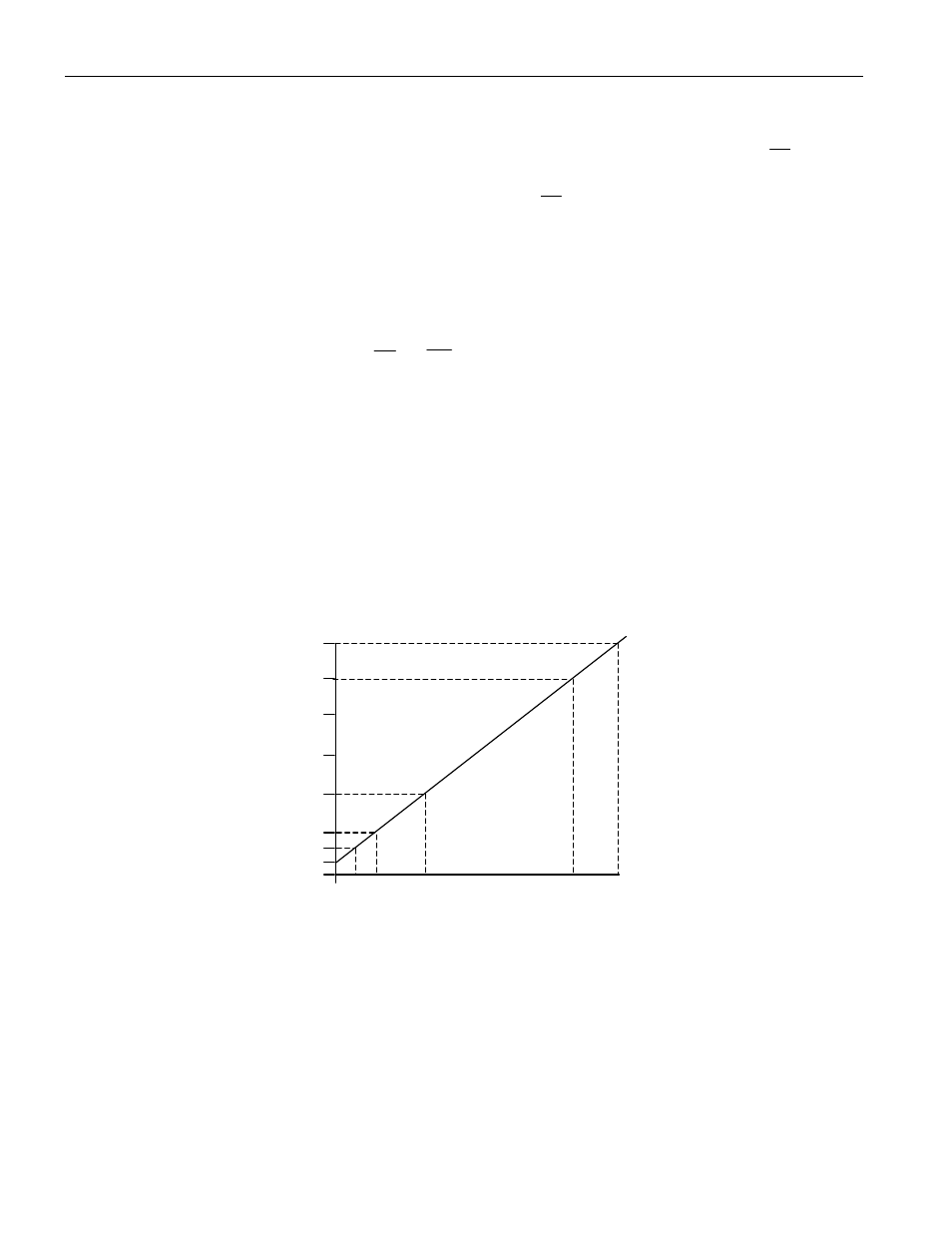
TYPICAL I
CC
VERSUS FREQUENCY
35
I
CC
mA
30
25
20
15
5
3
2
0 2 4
12
33
40 MHz XTAL
FREQUENCY