Maxim Integrated DS80C390 User Manual
Page 34
DS80C390
34 of 58
110199
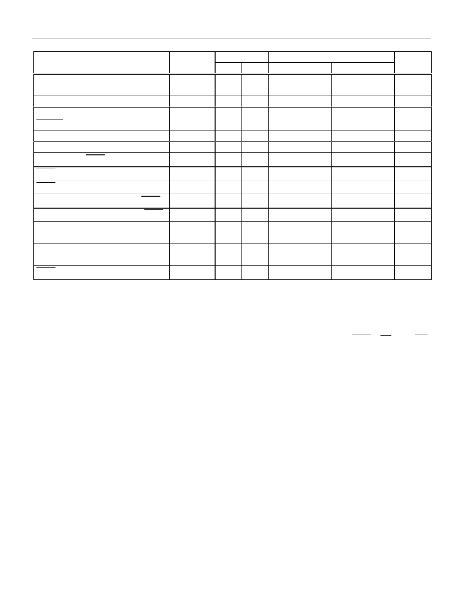
AC ELECTRICAL CHARACTERISTICS (Multiplexed address/data bus)
40 MHz
VARIABLE CLOCK
PARAMETER
SYMBOL MIN MAX
MIN
MAX
UNITS
Oscillator Freq.
(Ext. Osc)
1 / t
CLCL
0
40
0
40
MHz
(Ext. Crystal)
1
40
1
40
ALE Pulse Width
t
LHLL
0.375 t
MCS
- 5
ns
Port 0 Instruction Address or
4
CE0
−
Valid to ALE Low
t
AVLL
0.125 t
MCS
- 5
ns
Address Hold after ALE Low
t
LLAX1
0.125 t
MCS
- 5
ns
ALE Low to Valid Instruction In
t
LLIV
0.625 t
MCS
- 20
ns
ALE Low to
PSEN
Low
t
LLPL
0.125 t
MCS
- 5
ns
PSEN
Pulse Width
t
PLPH
0.5 t
MCS
- 5
ns
PSEN
Low to Valid Instruction In
t
PLIV
0.5 t
MCS
- 20
ns
Input Instruction Hold after
PSEN
t
PXIX
0
0
ns
Input Instruction Float after
PSEN
t
PXIZ
0.25 t
MCS
- 5
ns
Port 0 Address to Valid Instruction
In
t
AVIV1
0.75 t
MCS
- 20
ns
Port 2, 4 Address to Valid
Instruction In
t
AVIV2
0.875 t
MCS
- 25
ns
PSEN
Low to Address Float
t
PLAZ
0
0
ns
NOTES FOR AC ELECTRICAL CHARACTERISTICS:
1. All parameters apply to both commercial and industrial temperature operation unless otherwise noted.
2. The value t
MCS
is a function of the machine cycle clock in terms of the processor’s input clock
frequency. These relationships are described in the “Stretch Value Timing” table.
3. All signals characterized with load capacitance of 80 pF except Port 0, ALE,
PSEN
,
RD
and
WR
with 100 pF.
4. Interfacing to memory devices with float times (turn off times) over 25 ns may cause bus contention.
This will not damage the parts, but will cause an increase in operating current.
5. Specifications assume a 50% duty cycle for the oscillator. Port 2 and ALE timing will change in
relation to duty cycle variation.
6. Some AC timing characteristic drawings contain references to the CLK signal. This waveform is
provided to assist in determining the relative occurrence of events, and cannot be used to determine
the timing of signals relative to the external clock.