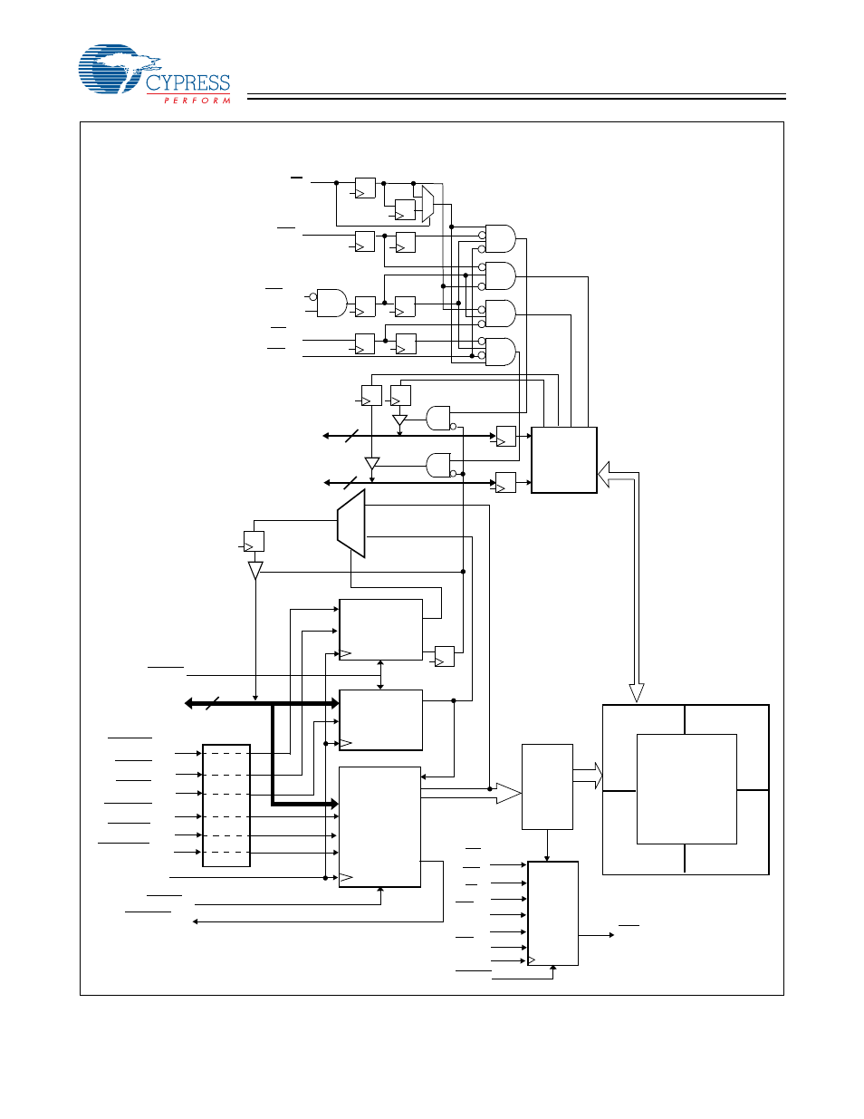
Port 1 operation-control logic block diagram – Cypress CY7C0430BV User Manual
Page 4
CY7C0430BV
CY7C0430CV
Document #: 38-06027 Rev. *B
Page 4 of 37
Addr.
Read
Port 1 Operation-Control Logic Block Diagram
R/W
P1
CE
0P1
CE
1P1
LB
P1
OE
P1
UB
P1
I/O
9P1
–I/O
17P1
I/O
0P1
–I/O
8P1
I/O
Control
Counter/
A
0P1
–A
15P1
CLK
P1
CNTLD
P1
CNTINC
P1
CNTRST
P1
16
9
9
MKLD
P1
CNTINT
P1
MKRD
P1
Mask Register
Port-1
Port 1
Port 1
64K × 18
QuadPort
DSE Array
Por
t 1
Po
rt 2
Port 4
Port 3
Address
Register
Readback
Register
Port 1
CNTRD
P1
Port 1
Address
Decode
Port 1
Interrupt
Logic
R/W
P1
CE
0P1
CE
1P1
OE
P1
INT
P1
CLK
P1
MRST
MRST
Priority
Decision
Logic
MRST
(Address Readback is independent of CEs)
W
LB
P1
UB
P1
This manual is related to the following products:
See also other documents in the category Cypress Hardware:
- CY7C1410AV18 (29 pages)
- CY7C1411JV18 (28 pages)
- CY7C1383FV25 (28 pages)
- CY14B256L (18 pages)
- CY7C1307BV25 (21 pages)
- CY7C1041DV33 (13 pages)
- CY62167EV18 (13 pages)
- Perform CY7C1565V18 (28 pages)
- STK11C68-5 (15 pages)
- 7C185-20 (11 pages)
- CY7C1168V18 (27 pages)
- CY7C1318CV18-250BZC (26 pages)
- CY7C1364C (18 pages)
- Perform CY7C1382D (34 pages)
- CY7C106D (11 pages)
- CY14E102N (21 pages)
- CY7C1418AV18 (31 pages)
- enCoRe CY7C638xx (83 pages)
- CY7C1018DV33 (9 pages)
- CY7C1292DV18 (23 pages)
- CY7C130 (19 pages)
- CY7C1424BV18 (30 pages)
- CY62157EV18 (12 pages)
- CY7C1392BV18 (31 pages)
- CY7C1302DV25 (18 pages)
- Perform CY7C1511KV18 (31 pages)
- West Bridge Astoria AN46860 (4 pages)
- CY7C1386FV25 (30 pages)
- CY7C1163V18 (29 pages)
- CY7C1266V18 (27 pages)
- CY7C1334H (13 pages)
- CY7C1018CV33 (7 pages)
- CY62136VN (12 pages)
- AN20639 (3 pages)
- CY7C1338G (17 pages)
- CY7C1462AV33 (27 pages)
- CY7C1145V18 (28 pages)
- STK11C88 (15 pages)
- CY7C1231H (12 pages)
- Perform CY7C142 (15 pages)
- CY14E256L (18 pages)
- STK15C88 (15 pages)
- CY7C1297H (15 pages)
- CY7C1441AV33 (31 pages)
- CapSense CY8C20x36 (34 pages)