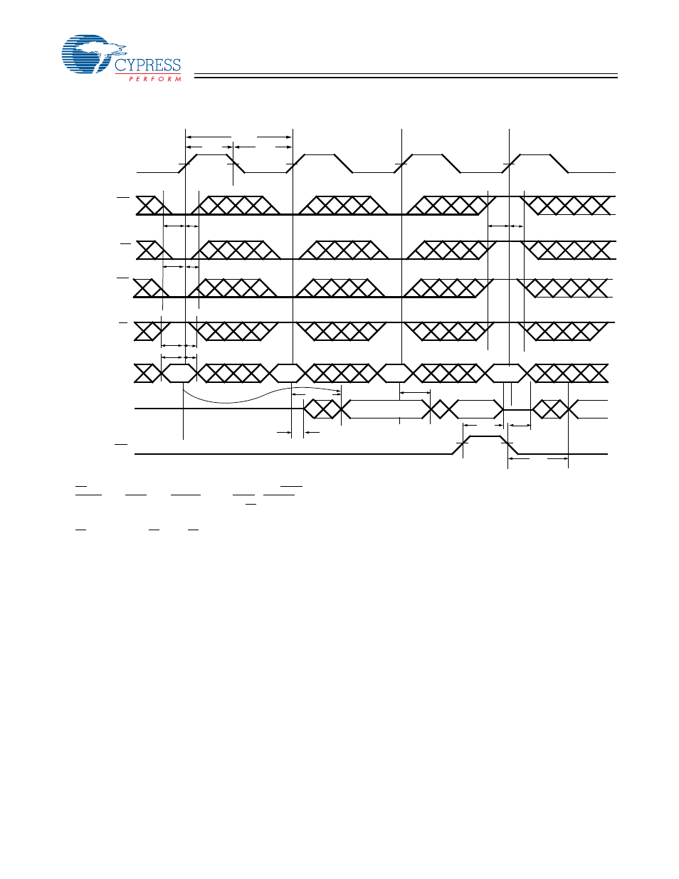
Switching waveforms – Cypress CY7C0430BV User Manual
Page 13

CY7C0430BV
CY7C0430CV
Document #: 38-06027 Rev. *B
Page 13 of 37
Read Cycle
[12, 13, 14, 15, 16]
Notes:
12. OE is asynchronously controlled; all other inputs (excluding MRST) are synchronous to the rising clock edge.
13. CNTLD = V
IL
, MKLD = V
IH
, CNTINC = x, and MRST = CNTRST = V
IH
.
14. The output is disabled (high-impedance state) by CE = V
IH
following the next rising edge of the clock.
15. Addresses do not have to be accessed sequentially. Note 13 indicates that address is constantly loaded on the rising edge of the CLK. Numbers are for reference
only.
16. CE is internal signal. CE = VIL if CE
0
= V
IL
and CE
1
= V
IH
.
Switching Waveforms
(continued)
t
CH2
t
CL2
t
CYC2
t
SC
t
HC
t
SW
t
HW
t
SA
t
HA
A
n
A
n+1
CLK
CE
R/W
ADDRESS
DATA
OUT
OE
A
n+2
A
n+3
t
SC
t
HC
t
OHZ
t
OE
t
OLZ
t
DC
t
CD2
t
CKLZ
Q
n
Q
n+1
Q
n+2
1 Latency
LB
UB
t
SB
t
HB
