11 camera serial interfaces (csi) interface, Camera serial interfaces (csi) interface – Kontron SMARC-sAT30 User Manual
Page 25
User’s Guide
25
3.2.11 Camera Serial Interfaces (CSI) Interface
The SMARC sAT30 module supports two dual lane CSI interfaces (named CSI0 and CSI1 according to the SMARC
Hardware specification). The SMARC four-lane CSI interface option is not supported. The camera interface
requirements are bound to the performance of the interfaces native to the NVIDIA Tegra T30 SoC.
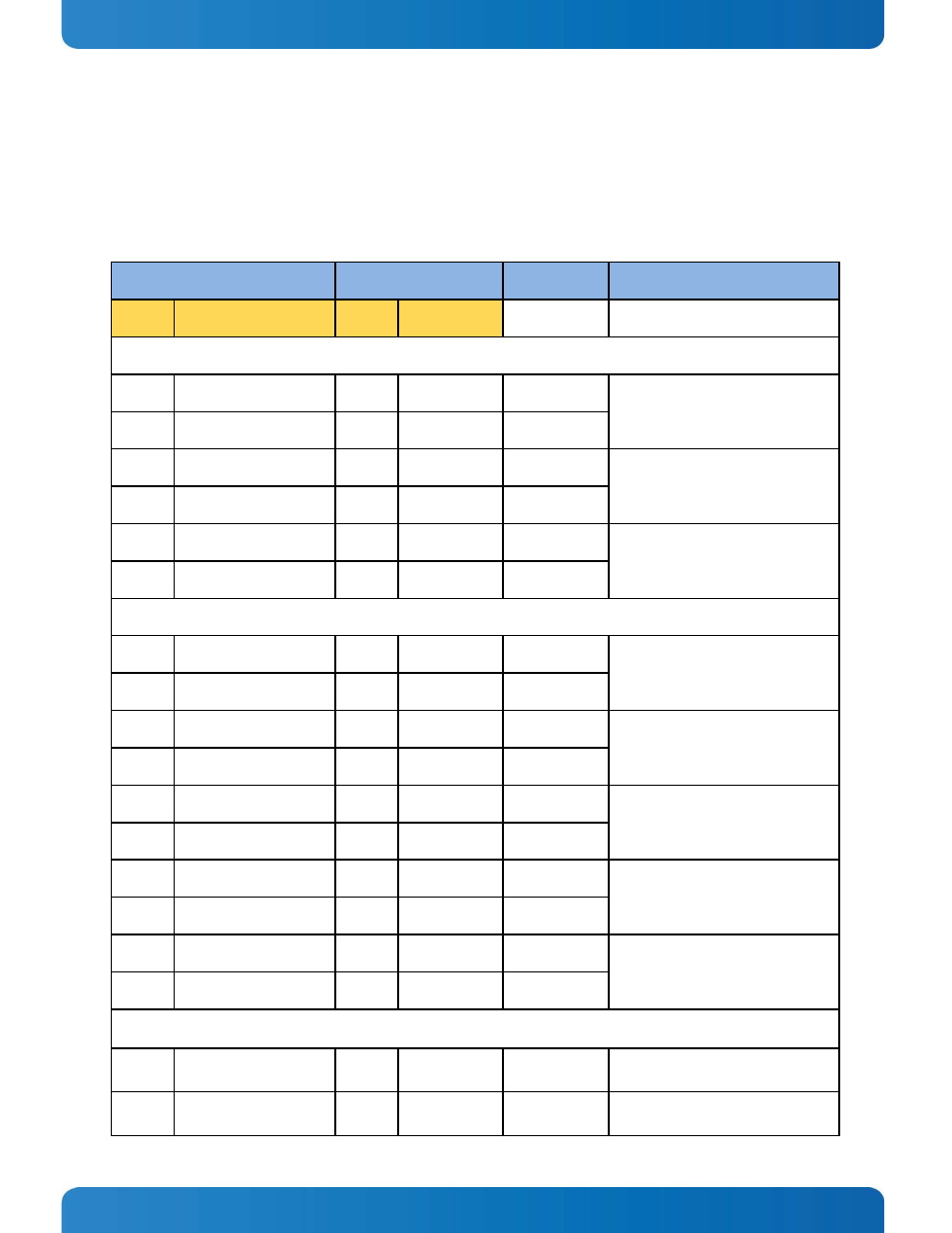
CSI interface signals are exposed on the SMARC sAT30 edge connector as shown below:
SMARC sAT30 Edge finger
NVIDIA T30 CPU
Net Name
Notes
Pin #
Pin Name
Pin #
Pin Name
CSI0 Camera Interface
S11
CSI0_D0+/PCAM_D12
AD2
CSI_D1AP
CSI0_D0A_P
CSI0 Differential data pair0 in
S12
CSI0_D0-/ PCAM_D13
AD3
CSI_D1AN
CSI0_D0A_N
S14
CSI0_D1+/PCAM_D14
AE3
CSI_D2AP
CSI0_D1A_P
CSI0 Differential data pair1 in
S15
CSI0_D1-/PCAM_D15
AE2
CSI_D2AN
CSI0_D1A_N
S8
CSI0_CK+/PCAM_D10
AD4
CSI_CLKAP
CSI0_CK_P
CSI0 Differential clock in
S9
CSI0_CK-/PCAM_D11
AC4
CSI_CLKAN
CSI0_CK_N
CSI1 Camera Interface
P7
CSI1_D0+ / PCAM_D2
AE1
CSI_D1BP
CSI1_D0B_P
CSI1 Differential data pair0 in
P8
CSI1_D0- / PCAM_D3
AD1
CSI_D1BN
CSI1_D0B_N
P10
CSI1_D1+ / PCAM_D4
AH1
CSI_D2BP
CSI1_D1B_P
CSI1 Differential data pair1 in
P11
CSI1_D1- / PCAM_D5
AH2
CSI_D2BN
CSI1_D1B_N
P13
CSI1_D2+ / PCAM_D6
Not used
P14
CSI1_D2- / PCAM_D7
P16
CSI1_D3+ / PCAM_D8
Not used
P17
CSI1_D3- / PCAM_D9
P3
CSI1_CK+ / PCAM_D0
AG2
CSI1_CK_P
CSI1 Differential clock in
P4
CSI1_CK- / PCAM_D1
AG3
CSI1_CK_N
CSI Camera support signals
S6
CAM_MCK
AD5
CAM_MCLK
CAM_MCLK
Master CLK out
S5
I2C_CAM_CK
AG5
CAM_I2C_SCL
I2C_CAM_CLK
I2C Camera support clock