7 lvds serialized lcd display interface, Figure 2: t30 module lvds lcd implementation, Lvds serialized lcd display interface – Kontron SMARC-sAT30 User Manual
Page 15
User’s Guide
15
T30 CPU
(U10)
AG9
AF16
AF10
AG11
T30_LCD_D[0:23]
T30_LCD_DE
T30_LCD_HSYNC
T30_LCD_VSYNC
T30_LCD_PCLK
H2
H1
G2
G1
LVDS
XMITTER
E2
(U25)
A3
TI
E1
SN75LVDS83B
A4
C2
B4
C1
A2
D2
D1
LCD_LVDS_Y0P
LCD_LVDS_Y0N
LCD_LVDS_Y1P
LCD_LVDS_Y1N
LCD_LVDS_Y2P
LCD_LVDS_Y2N
LCD_LVDS_Y3P
LCD_LVDS_Y3N
LCD_LVDS_CLKOUTP
LCD_LVDS_CLKOUTN
E
D
GE
F
IN
G
E
R
(J3
)
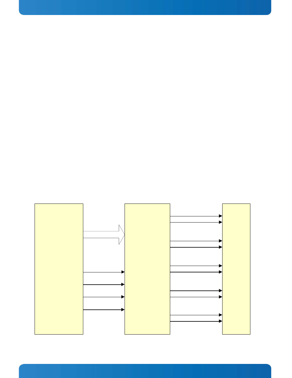
3.2.7 LVDS Serialized LCD Display Interface
LVDS LCD operation is not native to the NVIDIA Tegra SoC. The Module LVDS output is created on the Module from the
Tegra 24 bit LCD parallel data path. This is evident in the block diagram above (
). The LVDS color packing used on the Module is in the “18 bit color compatible mode” (more details on this
can be found later in this section and in the Ultra Low Power – Computer On Module Hardware Specification). The
display connection may be 18 bit or 24 bit, but if a 24 bit connection is used, then the display must be capable of
accepting an “18 bit color packing”. This is sometimes alternatively referred to as “6 bit pack” (it’s 6 bits per color, or
18 bits total …). For single channel LVDS, a display resolution up to approximately 1280 x 1024 may be supported
(approximate” because factors such as Carrier Board trace lengths, routing quality, cable length and quality, Carrier
EMI and ESD suppression device selections and display timing particulars can affect the maximum resolution
achieved). For high resolution displays (1280 x 1024 and higher), a Carrier Board based dual channel LVDS transmitter
operating from the Module parallel data path should be used instead. This is described in a later section.
For flat panel use, parallel LCD data and control information (Red, Green and Blue color data, Display Enable, Vertical
Synch and Horizontal Synch) are serialized onto a set of LVDS differential pairs. The information is packed into frames
that are 7 bits long. For 18 bit color depths, the data and control information utilize three LVDS channels (18 data bits
+ 3 control bits = 21 bits; hence 3 channels with 7 bit frames) plus a clock pair. For 24 bit color depths, four LVDS
channels are used (24 data bits + 3 control bits + 1 unused bit = 28 bits, or 4 x 7) plus a clock pair. The LVDS clock is
transmitted on a separate LVDS pair. The LVDS clock period is 7 times longer than the pixel clock period. The LVDS
clock edges are off from the 7 bit frame boundaries by 2 pixel periods. Unfortunately, there are two different 24 bit
color mappings in use. The more common one, sometimes referred to as “24 bit standard color mapping” is not
compatible with 18 bit panels, as it places the most significant RGB color data on the 4
th
LVDS data pair – the pair that
is not used on 18 bit panels. There is a less common “24 bit / 18 bit compatible” mapping that puts the least
significant color bits of the 24 bit set onto the 4
th
LVDS pair and allows 24 bit color depths.
S125
S126
S128
S129
S131
S132
S137
S138
S134
S135
Figure 2: T30 Module LVDS LCD Implementation