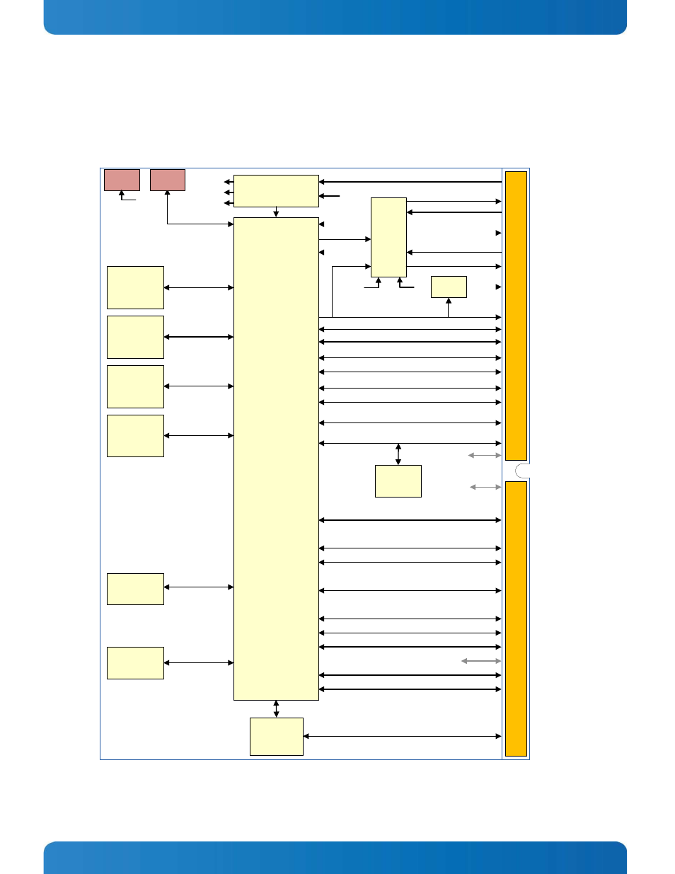
3 specifications, 1 functional block diagram, Figure 1: smarc sat30 block diagram – Kontron SMARC-sAT30 User Manual
Page 11: Specifications, Functional block diagram, 3specifications
User’s Guide
11
NVIDIA
Tegra T30
Quadcore
CPU
Boot Straps
Misc Ctrl Out
Misc Ctrl In
Pix Ck
I2C_
RGB LC
D Data and Control
HDMI
CSI- 2 (2 Pair)
CSI-2 (4-Pair)
GPIO (12 Bit) / PWM / Tach
UARTs (2x 2 Wire and 2x 4 Wire)
SDIO (4 Bit)
SDMMC
(4 bits used; SMARC supports up to 8)
I2C
(4 instances; one dedicated to Power Managemen
I2C_PM
N/C
CAN1
Serial
EEPROM
CAN0
N/C
SPI (2 instances)
I2S / DAP (3 instances)
SPDIF
SATA
USB / Host
USB2
USB / Host
USB1
USB OTG / Client
USB0
PCIe_C
N/C
PCIe x1 (plus support signals)
PCIE_B
PCIe x1 (plus support signals)
PCIE_A
3
Specifications
3.1
Functional Block Diagram
JTAG
Conn
JTAG
Conn
Various
Power
Power In (3.0V to 5.25V DC)
CPLD_JTAG
Module
Supplies
JTAG
Supplies
I2C_PM
CPLD
Misc
WDTO
Boot Device Select
Misc Ctrl Out
(Reset etc)
Misc Ctrl In
314 Pin 0.5mm
pitch edge finger
pattern for use with
MXM3 style carrier
2 G Byte SKU (4x 4Gbit)
1 G Byte SKU (4x 2Gbit)
DDR3 L
Logic
(Pwr Btn etc)
Dual Channel Pixel Clock
18 / 24 Bit
board connector
(aka the “SMARC
Carrier Connector”)
512M x 8
or
256M x 8
DDR3 L
512M x 8
or
256M x 8
DDR3 L
512M x 8
or
256M x 8
DDR3 L
512M x 8
or
256M x 8
DDR DQ31-DQ24
DDR DQ23-DQ16
DDR DQ15-DQ8
DDR DQ7-DQ0
GP CPLD_JTAG
S/N etc
LVDS
Xmiter
LVDS
t)
Actual pin order on
the connector will
differ from what is
implied here.
24 bit LVDS
requires
“18 bit compatible”
display
Interfaces shown in
gray and with N/C
designation are not
used on this
module but may be
used on other
modules
SPI Flash
8MB
GMI / SPI
eMMC
Flash Option
64GB Max
SDMMC
82mm x 50mm Form Factor
PCIe x1
Intel I210
(Springville)
GBE
Controller
MDI - 4 pairs for GBE
(plus support signals – LEDs, etc)
Figure 1: SMARC sAT30 Block Diagram