6 dma, 7 local bus / gpio, 1 local bus – Kontron COMe-bP5020 User Manual
Page 28: Local bus / gpio, Local bus, Serdes protocol mapping
www.kontron.com
28
User Guide
COMe-bP5020
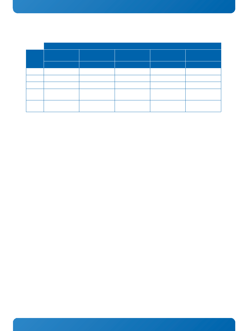
The following table illustrates the SerDes protocol combinations which can be selected by using the “sconf” command:
Table 9: SerDes Protocol Mapping
2.5.2.6 DMA
In order to support external application circuits which demand Direct Memory Access (DMA) the QorIQ™ CPU family provides
two external sets of control signals which are routed to the COM Express® connectors. For a more detailed description of the
DMA control signals please refer to the CPU’s reference manual
2.5.2.7 Local Bus / GPIO
2.5.2.7.1 Local Bus
The COMe-bP5020 provides a Local Bus interface for connecting directly to memory mapped parallel bus devices (SRAM-style).
The Local Bus implementation on the COMe-bP5020 supports 8-bit and 16-bit data signal paths depending on the Local Bus
chip select configuration and an 8 Mbyte address range for each of the two Local Bus chip selects.
Per default, LCS0# (LCS1# on the CPU) is configured for 16-bit operation, whereas LCS1# (LCS7# on the CPU) is configured for
8-bit operation.
The Local Bus signals designated as LAD0..15 incorporate multiplexed address and data information, whereby the Local Bus
signals LA16..31 are dedicated address lines. Please be aware that external address latches must be provided on the LAD8..15
lines if an address range greater than 64kB is to be addressed.
The numbering scheme for the Local Bus LA/LAD pins is noted in Power Architecture® style, meaning that LAD0 is the most
significant bit and LA31 is the least significant bit.
For a better understanding of the QorIQ™ P5020 Local Bus functionality and the involved control signals please refer to the
CPU’s reference manual.
CONNECTOR SIGNALS / CPU BANKS
BASE
CONFIG.
SERDES_
TX/RX[0..3]+/-
SERDES_
TX/RX[4..7]+/-
SERDES_
TX/RX[8..9]+/-
SERDES_
TX/RX[10..13]+/-
SERDES_
TX/RX[14..17]+/-
Bank1 A-D
Bank1 E-H
Bank1 I-J
Bank2 A-D
Bank3 A-D
1
PCIe1
PCIe2
Debug (Aurora)
4 x SGMII
--
2
PCIe1
PCIe2
Debug (Aurora)
4 x SGMII
XAUI
3
PCIe1
PCIe2
Debug (Aurora)
XAUI
--
4
SRIO2
(2.5 or 5 Gbps)
SRIO1
(2.5 or 5 Gbps)
Debug (Aurora)
4 x SGMII
--
5
SRIO2
(3.125 Gbps)
SRIO1
(3.125 Gbps)
Debug (Aurora)
4 x SGMII
--