Kontron COMe-bP5020 User Manual
Page 22
www.kontron.com
22
User Guide
COMe-bP5020
C28
LAD1
Local Bus
I/O-3.3
multiplexed CPU address/data signal
C29
N/C
N/C
C30
N/C
N/C
C31
GND
PWR
PWR
C32
LAD2
Local Bus
I/O-3.3
multiplexed CPU address/data signal
C33
LAD3
Local Bus
I/O-3.3
multiplexed CPU address/data signal
C34
LAD4
Local Bus
I/O-3.3
multiplexed CPU address/data signal
C35
LAD5
Local Bus
I/O-3.3
multiplexed CPU address/data signal
C36
LAD6
Local Bus
I/O-3.3
multiplexed CPU address/data signal
C37
LAD7
Local Bus
I/O-3.3
multiplexed CPU address/data signal
C38
LAD8 / GPIO0
Local Bus /
GPIO
I/O-3.3
weak PU when conf igured for
GPIO
multiplexed CPU address/data signal or
GPIO depending on SCONF setting
C39
LAD9 / GPIO1
Local Bus /
GPIO
I/O-3.3
weak PU when conf igured for
GPIO
multiplexed CPU address/data signal or
GPIO depending on SCONF setting
C40
LAD10 / GPIO2
Local Bus /
GPIO
I/O-3.3
weak PU when conf igured for
GPIO
multiplexed CPU address/data signal or
GPIO depending on SCONF setting
C41
GND
PWR
PWR
C42
LAD11 / GPIO3
Local Bus /
GPIO
I/O-3.3
weak PU when conf igured for
GPIO
multiplexed CPU address/data signal or
GPIO depending on SCONF setting
C43
LAD12 / GPIO4
Local Bus /
GPIO
I/O-3.3
weak PU when conf igured for
GPIO
multiplexed CPU address/data signal or
GPIO depending on SCONF setting
C44
LAD13 / GPIO5
Local Bus /
GPIO
I/O-3.3
weak PU when conf igured for
GPIO
multiplexed CPU address/data signal or
GPIO depending on SCONF setting
C45
LAD14 / GPIO6
Local Bus /
GPIO
I/O-3.3
weak PU when conf igured for
GPIO
multiplexed CPU address/data signal or
GPIO depending on SCONF setting
C46
LAD15 / GPIO7
Local Bus /
GPIO
I/O-3.3
weak PU when conf igured for
GPIO
multiplexed CPU address/data signal or
GPIO depending on SCONF setting
C47
EMI1_MDC
ETH MGT
O-2.5
Ethernet Management Clock
C48
EMI1_MDIO
ETH MGT
I/O-2.5
PU 3k3 2.5V
Ethernet Management In/Out
C49
IRQ1#
IRQ
I-3.3
PU 4k7 3.3V
C50
IRQ2#
IRQ
I-3.3
PU 4k7 3.3V
C51
GND
PWR
PWR
C52
SERDES_RX8+
SERDES
DP-I
AC coupled on module (100n)
SerDes Bank 1 I
C53
SERDES_RX8-
SERDES
DP-I
AC coupled on module (100n)
SerDes Bank 1 I
C54
T YPE0#
T YPE
PD 4k7
C55
SERDES_RX9+
SERDES
DP-I
AC coupled on module (100n)
SerDes Bank 1 J
C56
SERDES_RX9-
SERDES
DP-I
AC coupled on module (100n)
SerDes Bank 1 J
C57
T YPE1#
T YPE
C58
SERDES_RX10+
SERDES
DP-I
AC coupled on module (100n)
SerDes Bank 2A
C59
SERDES_RX10-
SERDES
DP-I
AC coupled on module (100n)
SerDes Bank 2A
C60
GND
PWR
C61
SERDES_RX11+
SERDES
DP-I
AC coupled on module (100n)
SerDes Bank 2B
C62
SERDES_RX11-
SERDES
DP-I
AC coupled on module (100n)
SerDes Bank 2B
C63
LA25
Local Bus
O-3.3
C64
LA24
Local Bus
O-3.3
C65
SERDES_RX12+
SERDES
DP-I
AC coupled on module (100n)
SerDes Bank 2C
C66
SERDES_RX12-
SERDES
DP-I
AC coupled on module (100n)
SerDes Bank 2C
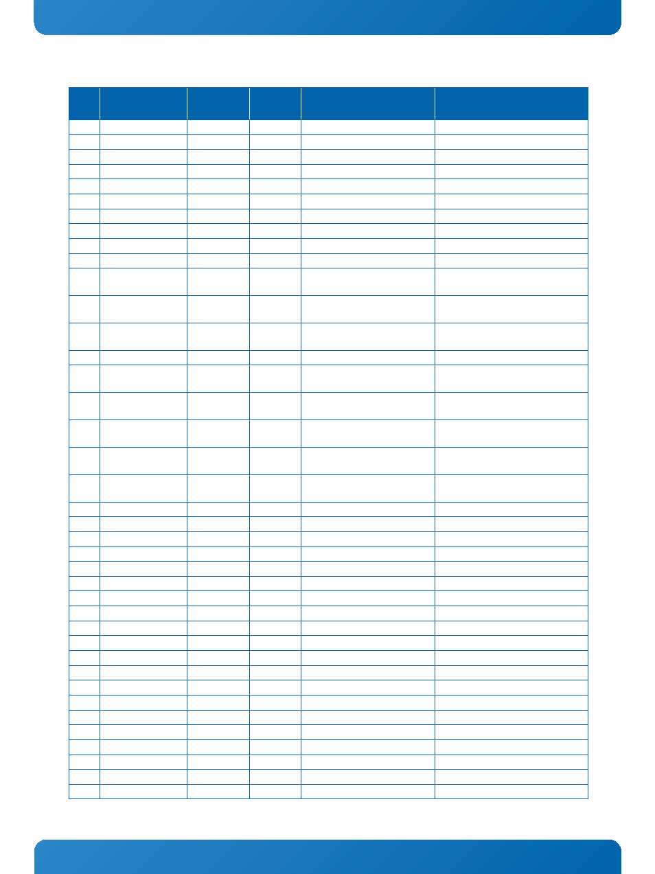
Table 6: Connector J2 Row C Pinout (cont’d)
PIN
SIGNAL
SIGNAL
GROUP
TYPE
TERMINATION
COMMENT