5 j8 jtag/debug interface, J8 jtag/debug interface - 13, Pinout of j8 - 13 – Kontron VMP3 User Manual
Page 47: 10 jtag/debug signal descriptions - 13, J8 - jtag/debug connector - 13, Vmp3 functional description
VMP3
Functional Description
ID 29230, Rev. 01
© 2005 Kontron Modular Computers GmbH
Page 2 - 13
29230
.01.UG.VC.050727/091424
P R E L I M I N A R Y
2.4.5
J8 JTAG/Debug Interface
This Test and Programming interface supports JTAG/Debug operations. This interface can be
used for connecting hardware emulators and debuggers (e.g. BDM, COP, …). It is comprised
of a set of ten signals whereby some are common to both interfaces and some are dedicated
to only one.
The following figure and tables provide pinout and signal information for this connector.
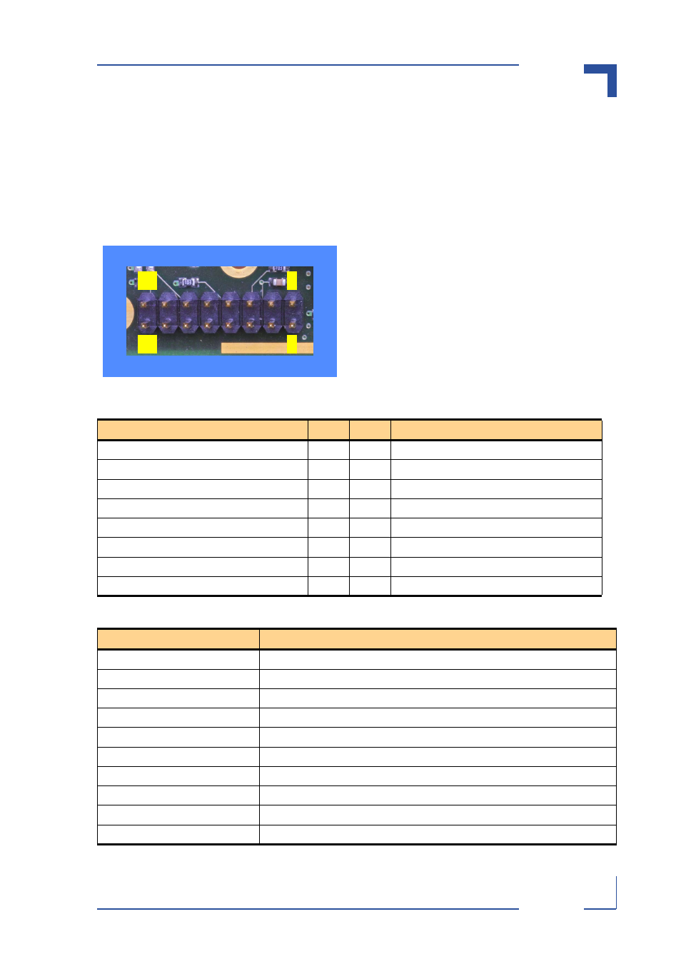
Figure 2-6: J8 - JTAG/Debug Connector
Table 2-9: Pinout of J8
SIGNAL
PIN
PIN
SIGNAL
TDO
1
2
NC
TDI
3
4
TRST
(pulled to +3.3V with 10 k
Ω
)
5
6
EMU_VCC
TCK
7
8
CHKSTP_IN (pulled to +3.3V with 10 k
Ω
)
TMS
9
10
NC
SRST
11
12
NC
HRST
13
14
NC
CHKSTP_OUT (pulled to +3.3V with 10 k
Ω
)
15
16
GND
Table 2-10: JTAG/Debug Signal Descriptions
SIGNAL
DESCRIPTION
TCK
Test Clock in for JTAG and emulator/debugger
TDI
Test Data In for JTAG and emulator/debugger
TDO
Test Data Out JTAG and emulator/debugger
TMS
Test Mode Select, input for JTAG and emulator/debugger
TRST
Test Reset, input for JTAG and emulator/debugger
HRST
Hard Reset, emulator/debugger hard reset input
SRST
Soft Reset, emulator/debugger reset input
CHKSTP_IN
Checkstop input
CHKSTP_OUT
Checkstop output
EMU_VCC
Reference Voltage of the JTAG/DEBUG core
1
2
16
15