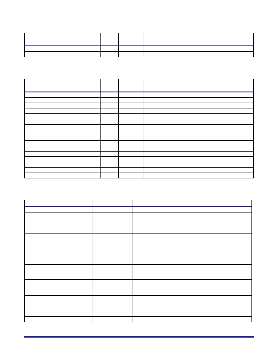
E table 2, Table 3 – Achronix Speedster22i Memory PHY User Manual
Page 9
UG043, April 26, 2014
9
Signal Name
Bus
Width
Direction
Description
phy_ctrli_dq/dqs_croe{a,b}
N/8
Input
Data a and b termination resistance enable signal for dq/dqs
phy_ctrlo_write_level_out
N/8
Output
Write leveling output for byte
Table 2: DDR PHY External Memory Interface Port List
Signal Name
Bus
Width
Direction
Description
sd_clk_p
3
Output
SDRAM differential clock signal (positive polarity)
sd_clk_n
3
Output
SDRAM differential clock signal (negative polarity)
sd_cke
4
Output
SDRAM clock enable control signal
sd_odt
4
Output
SDRAM on die termination control signal
sd_ras_n
1
Output
SDRAM RAS control signal
sd_cas_n
1
Output
SDRAM CAS control signal
sd_we_n
1
Output
SDRAM write enable control signal
sd_reset_n
1
Output
SDRAM reset signal
sd_a
16
Output
SDRAM address bus
sd_ba
3
Output
SDRAM bank select
sd_cs_n
4
Output
SDRAM chip select
sd_dm
N/8
Inout
SDRAM data mask
sd_dummy
N/8
Inout
Internal use only. Leave unconnected.
sd_dq
N
Inout
SDRAM data bus
sd_dqsn
N/8
Inout
SDRAM DQS bus, which is used to clock DQ bus
sd_dqsp
N/8
Inout
SDRAM DQS bus, which is used to clock DQ bus
Table 3: DDR PHY Parameter List
Parameter
Default (hex)
Valid Values
Description
DSIZE
16
Multiples of 8 up to 72
Local side data width
USE_CONTROLLER
`DEF_USE_CONTROLLER
`DEF_USE_CONTROLLER,
`DEF_NOT_USE_CONTROLLER
Specifies whether the hard controller
should be used in the design
NUM_CLK_OUTS
4
1 to 4
Number of clock outputs
NUM_RANKS
1
1 to 4
Number of memory ranks in system
BYPASS_TXRX_SD
`DEF_IO_RXSD_BYPASS_MUX
`DEF_IO_RXSD_BYPASS_MUX
`DEF_IO_RXSD_NO_BYPASS_MUX
Specifies data at full-rate vs half-rate
(Bypass=Full-rate, No_bypass=Half-rate)
EXTRA_PIPELINE_N
1'b1
1'b0, 1'b1
0 -> One extra clock cycle to load data
1 -> No extra cycle
Applies to both read and write paths
EXTRA_1CLK_DLY
0
0, 1
1 -> extra one clock delay in 2X mode.
WIDE_BUS
0
0, 1
1 -> Wide-bus used in fabric to convert
incoming data to quarter-rate. PHY
provides quarter-rate clock on clk_div4.
BYTE_LANE[N/8-1:0]_DLL_ADJ_DQ
6'h04
6’h00 to 6’hFF
DQ Slave adjust for BYTE_LANE
BYTE_LANE[N/8-1:0]_DLL_ADJ_DQS
6'h16
6’h00 to 6’hFF
DQS Slave adjust for BYTE_LANE
BYTE_LANE[N/8-1:0]_DLL_ADJ_DP
6'h04
6’h00 to 6’hFF
DP Slave adjust for BYTE_LANE
BYTE_LANE[N/8-
1:0]_WR_LVL_DQ_SELECT
`WLVL_SELECT_DQ0
`WLVL_SELECT_DQ0 up to
`WLVL_SELECT_DQ7
DQ bit used for write leveling
BYTE_LANE_DLL_DQSX9_CLK_ADJ
6'h10
6’h00 to 6’hFF
DLL adjust for wpb_tx_dqsx9_clk(0.25T)
BYTE_LANE_DLL_DQX9_CLK_ADJ
6'h30
6’h00 to 6’hFF
DLL adjust for wpb_tx_dqx9_clk(0.75T)
BYTE_LANE_CAC_DLL_ADJ_DQSN
6'h17
6’h00 to 6’hFF
DP Slave adj for CAC byte lanes (0.35T)