Phy structure and operation, Ddr phy up to x9 – Achronix Speedster22i Memory PHY User Manual
Page 10
10
UG043, April 26, 2014
PHY Structure and Operation
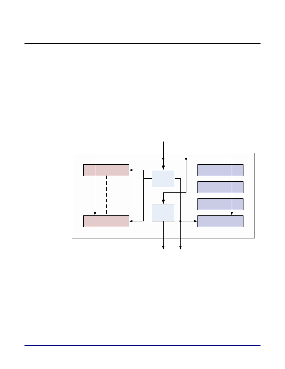
Figure 5 below illustrates a high level overview of the DDR PHY structure. It consists of up to
9 data byte lanes, each implementing a x8 interface to give a max width of x72. There are also
4 byte lanes to implement Control, Address, Command (CAC) functions. Three of the CAC
byte lanes operate at full rate mode and one of them operates in half-rate mode (denoted by
the extension SD).
The full-rate clock typically (but not necessarily) comes from the PLL and then goes through
two clock dividers, one implementating a divide-by-2 and the other implementing a divide-
by-4. The full-rate clock goes to all byte lanes; the divide-by-2 clock is fed into the byte-lanes
that have half-rate operation; and the divide-by-4 clock is actually only transmitted to the
fabric since the half-rate to quarter-rate conversion is not done in the PHY, but rather has to
be done in the fabric (refer to the PHY – Controller Interfacing through Widebus section of
the document for details on this).
Data Byte Lane
Data Byte Lane
CAC Byte Lane
CAC Byte Lane
CAC Byte Lane
CAC Byte Lane SD
Clk Divider
(/2)
Clk Divider
(/4)
Clk from PLL
Clocks to fabric
Clk_div2
Clk_div4
Clk_div2
DDR PHY
Up to x9
Clk
Clk
Clk_div2
Clk
Figure 5: DDR PHY Structure