Table 1 – Achronix Speedster22i Memory PHY User Manual
Page 8
8
UG043, April 26, 2014
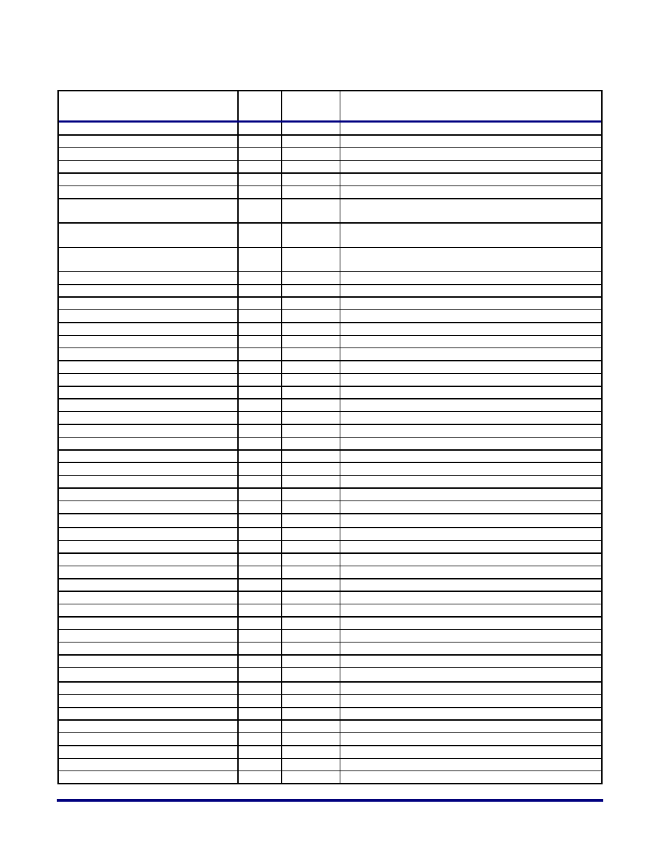
Table 1: DDR PHY – Hard/Soft Controller Interface Port List
Signal Name
Bus
Width
Direction
Description
clk
1
Input
User reference clock (full-rate), generally coming in from a PLL
reset_n
1
Input
Active-low user reset
phy_ddr_clk_en
1
Input
Clk enable signal for CAC byte lane to enable clocking
byte_{3,2,1,0}_from_ctrl_{a,b}
10
Input
Input to the CAC byte lanes
clk_div2
1
Output
Half-rate clock output from PHY, synchronous to clk
clk_div4
1
Output
Quarter-rate clock output from PHY, synchronous to clk
phy_ci_dq{a,b,c,d}
N
Input
Four sets of dq data signals for TX interface: all used in half-rate,
a and b only used in full-rate
phy_ci_dq{a,b,c,d}8
N/8
Input
Four sets of dq mask signals for Tx interface: all used in half-rate,
a and b only used in full-rate
phy_co_dq{a,b,c,d}
N
Output
Four sets of dq data signals from RX interface: all used in half-
rate, a and b only used in full-rate
phy_ctrli_dq{a,b}9
1
Input
Data bits for the preamble
phy_ctrli_dqsa
1
Input
DQS input into the byte
phy_co_l_busy_align
9
Output
Busy alignment output signal for byte
phy_co_l_d_req
9
Output
Data request output for byte
phy_co_l_d_req_align
9
Output
Data request output for byte when widebus is enabled
phy_co_l_d_req_early_align
9
Output
Data request early output for byte when widebus is enabled
phy_co_l_r_valid
9
Output
Read valid output for byte
phy_co_l_r_valid_align
9
Output
Read valid output for byte when widebus is enabled
phy_co_l_r_valid_early_align
9
Output
Read valid early output for byte when widebus is enabled
phy_ctrli_write_level_en
N/8
Input
Enable signal for write leveling
phy_ctrli_doing_wr_level
1
Input
Indicator of write leveling
phy_ctrli_l_busy
9
Input
Busy signal input
phy_ctrli_dreq_early
9
Input
Early data request input
phy_ctrli_rvalid_early
9
Input
Early read valid signal input
phy_ci_{rd,wr}req
1
Input
Read/Write request input
phy_ctrlo_{rd,wr}req
1
Output
Read/Write request output
dbg_dqs_{a,b}
9
Output
Debug signal for dqs output from IO registers
dbg_dq9_bit_{a,b}
9
Output
Debug signal for dq9 output from IO registers
phy_ctrli_l_io_recal
1
Input
DDR update after recalibration for io comp block
Soft Controller (Fabric) Interface
phy_ci_dq/dqs_add_dly
N/4
Input
2-bit value per byte to add delay to dq/dqs path
phy_ci_dreq
9
Input
Data request input
phy_ci_l_r_valid
9
Input
Read valid signal input
phy_ci_rd_en
N/8
Input
Read enable input
phy_ci_rd_rstn
N/8
Input
Active low read reset
phy_ci_sd_dq_ptr_rstn
N/8
Input
Active low reset for pointer in deserializer logic
phy_ci_slave_adj
8
Input
Slave DLL delay adjustment
phy_ci_slave_dqsn_en
N/8
Input
Active low dqs enable in the slave DLL
phy_ci_dq/dqs_cdoe{a,b}
N/8
Input
Data a and b output enable signal for dq/dqs
phy_ci_dq/dqs_croe{a,b}
N/8
Input
Data a and b termination resistance enable signal for dq/dqs
phy_co_write_level_out
N/8
Output
Write leveling output for byte
Hard Controller Interface
phy_ctrli_dq/dqs_add_dly
N/4
Input
2-bit value per byte to add delay to dq/dqs path
phy_ctrli_dreq
9
Input
Data request input
phy_ctrli_l_r_valid
9
Input
Read valid signal input
phy_ctrli_rd_en
N/8
Input
Read enable input
phy_ctrli_rd_rstn
N/8
Input
Active low read reset
phy_ctrli_slave_adj
8
Input
Slave DLL delay adjustment
phy_ctrli_slave_en
12
Input
Enable signal for the slave DLL
phy_ctrli_dq/dqs_cdoe{a,b}
N/8
Input
Data a and b output enable signal for dq/dqs